Citations
This panel presents information regarding the papers that have cited the interatomic potential (IP) whose page you are on.
The OpenKIM machine learning based Deep Citation framework is used to determine whether the citing article actually used the IP in computations (denoted by "USED") or only provides it as a background citation (denoted by "NOT USED"). For more details on Deep Citation and how to work with this panel, click the documentation link at the top of the panel.
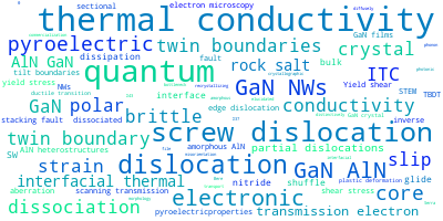
The word cloud to the right is generated from the abstracts of IP principle source(s) (given below in "How to Cite") and the citing articles that were determined to have used the IP in order to provide users with a quick sense of the types of physical phenomena to which this IP is applied.
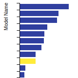
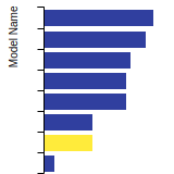
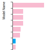
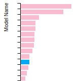
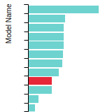
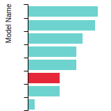
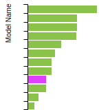
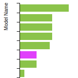
The bar chart shows the number of articles that cited the IP per year. Each bar is divided into green (articles that USED the IP) and blue (articles that did NOT USE the IP).
Users are encouraged to correct Deep Citation errors in determination by clicking the speech icon next to a citing article and providing updated information. This will be integrated into the next Deep Citation learning cycle, which occurs on a regular basis.
OpenKIM acknowledges the support of the Allen Institute for AI through the Semantic Scholar project for providing citation information and full text of articles when available, which are used to train the Deep Citation ML algorithm.
|
This panel provides information on past usage of this interatomic potential (IP) powered by the OpenKIM Deep Citation framework. The word cloud indicates typical applications of the potential. The bar chart shows citations per year of this IP (bars are divided into articles that used the IP (green) and those that did not (blue)). The complete list of articles that cited this IP is provided below along with the Deep Citation determination on usage. See the Deep Citation documentation for more information.
92 Citations (62 used)
Help us to determine which of the papers that cite this potential actually used it to perform calculations. If you know, click the .
USED (high confidence) Q. Wang, X. Wang, X. Liu, and J. Zhang, “Interfacial engineering for the enhancement of interfacial thermal conductance in GaN/AlN heterostructure,” Journal of Applied Physics. 2021. link Times cited: 14 Abstract: Effective heat dissipation is the bottleneck problem for the… read moreAbstract: Effective heat dissipation is the bottleneck problem for the development and commercialization of GaN-based high-power electronic and photonic devices. To address this challenge and explore the underlying mechanism of phonon transportation across the GaN/AlN heterointerface, in this work, we formed three types of GaN/AlN heterostructures with distinctively different interfacial morphologies by annealing recrystallization approach. It is found that the interfacial thermal conductance (ITC) of GaN/AlN heterostructures can be remarkably improved by tailoring the interfacial crystal structure and phase morphology. Besides the commonly amorphous phase and ideal ordered wurtzite phase, we further found that AlN may present an additional stable rock salt phase at the interfacial region, and its significant effect on interfacial thermal transport has been observed. Using molecular dynamics simulation, we systematically investigated the effects of different GaN/AlN heterojunctions on the ITCs. Our results suggest that heat dissipation at the GaN/AlN interface is dominated by phonons scattered diffusely by the amorphous region at interfaces and the ITC can be significantly enhanced by recrystallizing the amorphous AlN to rock salt one. Furthermore, through phonon vibrational spectrum, we revealed that phonon modes dominate the energy transport across the interfaces of wurtzite AlN/GaN, amorphous AlN/GaN, and rock salt AlN/GaN are significantly different. Finally, we found the ITC increased with the temperature due to the enhanced inelastic phonon scattering and the presence of additional excited phonon modes at higher temperatures. The findings elucidated here provide a clearer insight into the effect of interfacial microstructures on the interfacial thermal resistance of GaN–substrate interface, which also provide a viable heat management strategy for the high-power GaN-based devices. read less USED (high confidence) I. Belabbas, L. Pizzagalli, J. Kioseoglou, and J. Chen, “Core properties and the role of screw dislocations in the bulk n-type conductivity in InN.,” Physical chemistry chemical physics : PCCP. 2019. link Times cited: 1 Abstract: First principles calculations, based on density functional t… read moreAbstract: First principles calculations, based on density functional theory, have been carried out to investigate the role of screw dislocations in the bulk n-type conductivity which is usually observed in indium nitride. Energetics, atomic and electronic structures of different core configurations of dislocations, running along the [0001] polar or along the [112[combining macron]0] non-polar direction, have been determined and compared. This enabled inspection of the modifications in the properties of screw dislocations when the growth direction is changed. For the c-type screw dislocation, the configuration with a double 6-atom ring, involving wrong bonds was revealed as a ground state configuration, and for the a-type screw dislocation, the shuffle configuration was found to be energetically favoured over glide ones. Unlike core configurations of the a-type screw dislocation, those of the c-type screw dislocation have their Fermi levels pinned in the conduction band and thus act as a source of non-intentional n-type conductivity. This demonstrates that eliminating the contribution of screw dislocations to the n-type conductivity can be achieved by growing wurtzite InN along the non-polar direction. read less USED (high confidence) W. Fu and H. W. Choi, “Designing microstructures for bandgap manipulation of InGaN Quantum Wells by k.p simulation coupled with molecular dynamics,” 2018 International Conference on Numerical Simulation of Optoelectronic Devices (NUSOD). 2018. link Times cited: 0 Abstract: In this work, we present the design of InGaN microstructures… read moreAbstract: In this work, we present the design of InGaN microstructures by manipulation of quantum well bandgap via strain engineering. By coupling strain field extracted from molecular dynamics simulation to k.p simulation, we are able to associate the effect of geometry and strain of a structure to its light emission. read less USED (high confidence) X. W. Zhou and S. Foiles, “Uncertainty Quantification and Reduction of Molecular Dynamics Models.” 2017. link Times cited: 9 Abstract: Molecular dynamics (MD) is an important method underlying th… read moreAbstract: Molecular dynamics (MD) is an important method underlying the modern field of Computational Materials Science. Without requiring prior knowledge as inputs, MD simulations have been used to study a variety of material problems. However, results of molecular dynamics simulations are often associated with errors as compared with experimental observations. These errors come from a variety of sources, including inac- curacy of interatomic potentials, short length and time scales, idealized problem description and statistical uncertainties of MD simulations themselves. This chapter specifically devotes to the statistical uncertainties of MD simulations. In particular, methods to quantify and reduce such statistical uncertainties are demonstrated using a variety of exemplar cases, including calculations of finite temperature static properties such as lattice constants, cohesive energies, elastic constants, dislocation energies, ther- mal conductivities, surface segregation and calculations of kinetic properties such as diffusion parameters. We also demonstrate that when the statistical uncertainties are reduced to near zero, MD can be used to validate and improve widely used theories. read less USED (high confidence) J. Zhang and C. Wang, “Size-dependent pyroelectric properties of gallium nitride nanowires,” Journal of Applied Physics. 2016. link Times cited: 14 Abstract: The size scale effect on the pyroelectricproperties is studi… read moreAbstract: The size scale effect on the pyroelectricproperties is studied for gallium nitride(GaN) nanowires (NWs) based on molecular dynamics simulations and the theoretical analysis. Due to the significant influence of the surface thermoelasticity and piezoelectricity at the nanoscale, the pyroelectric coefficient of GaN NWs is found to depend on the cross-sectional size. This size-dependent pyroelectric coefficient of GaN NWs together with the size-dependent dielectric constant reported in our previous study is employed to study the pyroelectric potential of GaN NWs subjected to heating. The results show that the size scale effect is significant for thin NWs (cross-sectional size in nanometers) and may raise the pyroelectric potential of GaN NWs by over 10 times. Such a size scale effect on the pyroelectricproperties of NWs originates from the influence of thermoelasticity, piezoelectricity, and dielectricity at the nanoscale and decreases with increasing cross-section of GaN NWs. It is expected that the present study may have strong implication in the field of energy harvesting at the nanoscale, as pyroelectricity offers a new avenue to the design of novel nanogenerators. read less USED (high confidence) A. Gielen and F. V. McKenzie, “Thermo-mechanical challenges for quantum devices,” Proceedings of the 5th Electronics System-integration Technology Conference (ESTC). 2014. link Times cited: 1 Abstract: In the last few years Technical University of Delft, under l… read moreAbstract: In the last few years Technical University of Delft, under leadership of Prof.dr.ir. Leo Kouwenhoven, has developed several successful concepts for quantum devices that are suitable for quantum computing and quantum communication. From a quantum research point of view we are still in a very fundamental state, several practical issues already arise that are also important to a successful application and industrialization of quantum computing and communication. This paper will focus on these application issues. The quantum devices have the following challenges: (1) thousands to millions of the basic quantum manipulator, referred to as QuBit, must be connected to the outside (conventional electronic) world; (2) the circuits must be made stable and reproducible; (3) the excitation and control of the quantum states requires advanced low-power RF based control electronics; (4) they need to operate at very low (1K or less) to enable superconductivity that provides the right environment to induce the quantum states, as well as to minimize thermal energy interference of the quantum states. As the quantum device under investigation is built from nano-wires and thin metal films and operates at near zero [K], material properties will deviate typical bulk values at room temperature. Atomistic simulations are used to estimate these values and obtain insight into the mechanical behavior of the wire. A continuum model, that uses results of the atomistic simulations is used to obtain insight into the thermo-mechanical loading of the quantum devices due to cool down to the operating temperature of near zero Kelvin. read less USED (high confidence) M. K. Horton, S. Rhode, and M. Moram, “Structure and electronic properties of mixed (a + c) dislocation cores in GaN,” Journal of Applied Physics. 2014. link Times cited: 13 Abstract: Classical atomistic models and atomic-resolution scanning tr… read moreAbstract: Classical atomistic models and atomic-resolution scanning transmission electron microscopy studies of GaN films reveal that mixed (a + c)-type dislocations have multiple different core structures, including a dissociated structure consisting of a planar fault on one of the {1 2¯10} planes terminated by two different partial dislocations. Density functional theory calculations show that all cores introduce localized states into the band gap, which affects device performance. read less USED (high confidence) P. Hirsch et al., “The dissociation of the [a + c] dislocation in GaN,” Philosophical Magazine. 2013. link Times cited: 33 Abstract: In 1952, Cottrell proposed that the Lomer dislocation formed… read moreAbstract: In 1952, Cottrell proposed that the Lomer dislocation formed by interaction of two glide dislocations in a fcc crystal could transform into an immobile dislocation by dissociation into partial dislocations bounding a stacking fault, causing a block to further slip, a concept important in work hardening. Evidence for this and many other dissociations has been provided by the diffraction contrast technique and in particular by its ‘weak beam’ variant, which has a resolution limit of about 15 angstroms. Today, with the advent of aberration corrected microscopes it is possible to determine directly the atomic structure of the faults and partial dislocations. In this paper, we describe the results of a study using the High Angle Angular Dark Field technique (HAADF) in an aberration corrected scanning transmission electron microscope (STEM), of the dissociation of the [a + c] dislocations in (0 0 0 1) GaN films grown on sapphire substrates. The dislocations are found to be inclined with respect to the c-axis, but optical sectioning imaging methods allow the structure to be determined and an estimate of the tilt angle to be made. The dislocations are found to be dissociated by climb and glide on the a plane and the STEM results, and structural arguments supported by theoretical calculations suggest that the dissociation reaction is [a + c] = 1/2[a + c] + 1/2[a + c] + fault. The structure of the fault is found to be similar to that identified in 1965 by Drum in AlN but frequently modified by steps due to kinks in the inclined dislocation. read less USED (high confidence) D. Spiteri, J. Pomeroy, and M. Kuball, “Influence of microstructural defects on the thermal conductivity of GaN: A molecular dynamics study,” physica status solidi (b). 2013. link Times cited: 14 Abstract: The lattice thermal conductivity is known to depend on cryst… read moreAbstract: The lattice thermal conductivity is known to depend on crystal quality, but the reduction in thermal conductivity due to specific defects is presently unclear. Molecular dynamics simulations were used to investigate the impact of microstructural defects on the thermal conductivity of gallium nitride. The conductivity of a finite crystal was reduced to (39 ± 4)% by a screw dislocation density of 2.0 × 1013 cm−2 and to (51 ± 4)% by an edge dislocation of similar density, illustrating that the type of dislocation is important for thermal conductivity. The effect of stacking faults on thermal conductivity was also investigated. read less USED (high confidence) M. Fujikane, T. Yokogawa, S. Nagao, and R. Nowak, “Strain Rate Controlled Nanoindentation Examination and Incipient Plasticity in Bulk GaN Crystal,” Japanese Journal of Applied Physics. 2013. link Times cited: 7 Abstract: Yield shear stress dependence on dislocation density and cry… read moreAbstract: Yield shear stress dependence on dislocation density and crystal orientation was studied in bulk GaN crystals by nanoindentation examination. The yield shear stress decreased with increasing dislocation density, and it decreased with decreasing nanoindentation strain-rate. It reached and coincided at 11.5 GPa for both quasi-static deformed c-plane (0001) and m-plane (101̄0) GaN. Taking into account theoretical Peierls–Nabarro stress and yield stress for each slip system, these phenomena were concluded to be an evidence of heterogeneous mechanism associated plastic deformation in GaN crystal. Transmission electron microscopy and molecular dynamics simulation also supported the mechanism with obtained r-plane (1̄012) slip line right after plastic deformation, so called pop-in event. The agreement of the experimentally obtained atomic shuffle energy with the calculated twin boundary energy suggested that the nucleation of the local metastable twin boundary along the r-plane concentrated the indentation stress, leading to an r-plane slip. read less USED (high confidence) J. N. Sarma, R. Chowdhury, and R. Jayaganthan, “Molecular dynamics investigation of the thermomechanical behavior of monolayer GaN,” Journal of Applied Physics. 2013. link Times cited: 8 Abstract: Molecular dynamics simulations are performed on monolayer ga… read moreAbstract: Molecular dynamics simulations are performed on monolayer gallium nitride to study their mechanical behavior at various temperatures in the range of 10 to 1700 K. The transition from brittle to ductile nature has been illustrated from the evolution of fracture at two different temperatures of 700 and 1300 K. Brittle to ductile transition temperatures TBDT are obtained from the plots of logarithm of yield stress and inverse temperature at different strain rates and compared qualitatively with the same system in the presence of single and diatomic vacancies. Logarithm of strain rate against inverse of TBDT thus obtained represents an Arrhenius plot, the slope of which corresponds to the activation energy of dislocation glide that is found to be approximately 2.0 ± 0.05 eV for the present case. This suggests that the brittle to ductile transition is controlled by the dislocation mobility as in the case of other semiconductors like silicon and germanium. This behavior is found to be consistent with the presen... read less USED (high confidence) X. Zhou and R. E. Jones, “Effects of nano-void density, size and spatial population on thermal conductivity: a case study of GaN crystal,” Journal of Physics: Condensed Matter. 2012. link Times cited: 9 Abstract: The thermal conductivity of a crystal is sensitive to the pr… read moreAbstract: The thermal conductivity of a crystal is sensitive to the presence of surfaces and nanoscale defects. While this opens tremendous opportunities to tailor thermal conductivity, true ‘phonon engineering’ of nanocrystals for a specific electronic or thermoelectric application can only be achieved when the dependence of thermal conductivity on the defect density, size and spatial population is understood and quantified. Unfortunately, experimental studies of the effects of nanoscale defects are quite challenging. While molecular dynamics simulations are effective in calculating thermal conductivity, the defect density range that can be explored with feasible computing resources is unrealistically high. As a result, previous work has not generated a fully detailed understanding of the dependence of thermal conductivity on nanoscale defects. Using GaN as an example, we have combined a physically motivated analytical model and highly converged large-scale molecular dynamics simulations to study the effects of defects on thermal conductivity. An analytical expression for thermal conductivity as a function of void density, size, and population has been derived and corroborated with the model, simulations, and experiments. read less USED (low confidence) H. Liu et al., “Investigation of edge effect on wurtzite gallium nitride in nanoindentation using molecular dynamics simulation,” Materials Today Communications. 2024. link Times cited: 0 USED (low confidence) L. Duan, S.-R. Tan, Y. Liu, and J. Guo, “Influence of irradiation-induced point defects on nanotribological properties of m-plane GaN investigated using molecular dynamics simulation,” Materials Today Communications. 2023. link Times cited: 0 USED (low confidence) X. Chen, W. Shao, N. Q. Le, and P. Clancy, “Transferable Force Field for Gallium Nitride Crystal Growth from the Melt Using On-The-Fly Active Learning.,” Journal of chemical theory and computation. 2023. link Times cited: 0 Abstract: Atomic-scale simulations of reactive processes have been sty… read moreAbstract: Atomic-scale simulations of reactive processes have been stymied by two factors: the lack of a suitable semiempirical force field on one hand and the impractically large computational burden of using ab initio molecular dynamics on the other hand. In this paper, we use an "on-the-fly" active learning technique to develop a nonparameterized force field that, in essence, exhibits the accuracy of density functional theory and the speed of a classical molecular dynamics simulation. We developed a force field capable of capturing the crystallization of gallium nitride (GaN) during a novel additive manufacturing process featuring the reaction of liquid Ga and gaseous nitrogen precursors to grow crystalline GaN thin films. We show that this machine learning model is capable of producing a single force field that can model solid, liquid, and gas phases involved in the process. We verified our computational predictions against a range of experimental measurements relevant to each phase and against ab initio calculations, showing that this nonparametric force field produces properties with excellent accuracy as well as exhibits computationally tractable efficiency. The force field is capable of allowing us to simulate the solid-liquid coexistence interface and the crystallization of GaN from the melt. The development of this transferable force field opens the opportunity to simulate the liquid-phase epitaxial growth more accurately than before to analyze reaction and diffusion processes and ultimately to establish a growth model of the additive manufacturing process to create the gallium nitride thin films. read less USED (low confidence) P. Zhao et al., “Investigation on nano-grinding process of GaN using molecular dynamics simulation: Nano-grinding parameters effect,” Journal of Manufacturing Processes. 2023. link Times cited: 2 USED (low confidence) Y. Xu, G. Sun, Z. Wan, D. Xu, and X. Luo, “Theoretical study on the thermal transport and its tunability of a-plane trilayer GaN,” Physica Scripta. 2023. link Times cited: 0 Abstract: Two-dimensional (2D) a-plane gallium nitride, a non-layered … read moreAbstract: Two-dimensional (2D) a-plane gallium nitride, a non-layered 2D material, has promising applications in photoelectric nanodevices due to its direct band bandgap. Herein, employing molecular dynamics simulations, we studied the thermal transport properties of a-plane trilayer GaN, and the temperature, together with strain modulation on the thermal conductivity of the system. The a-plane trilayer GaN shows anisotropic thermal conductivity with 70.22 Wm−1K−1 and 41.81 Wm−1K−1 along zigzag- and armchair- directions respectively at room temperature when extrapolated to infinite size. In addition, the thermal conductivity of trilayer GaN exhibits decreasing trend in response to the increase of temperature. The thermal conductivity decreases monotonically with the increased compressive uniaxial and biaxial strain, while it shows an up-then-down trend under tensile strain. The tunability of thermal conductivity under biaxial strain is much larger than that of uniaxial strain. The phonon density of states is further investigated to understand the behavior of thermal conductivity. The tunability of the system thermal conductivity will expand its applications in thermal management and nanodevices. read less USED (low confidence) Q. Peng, Z. Ma, S. Cai, S. Zhao, X. Chen, and Q. Cao, “Atomistic Insights on Surface Quality Control via Annealing Process in AlGaN Thin Film Growth,” Nanomaterials. 2023. link Times cited: 1 Abstract: Aluminum gallium nitride (AlGaN) is a nanohybrid semiconduct… read moreAbstract: Aluminum gallium nitride (AlGaN) is a nanohybrid semiconductor material with a wide bandgap, high electron mobility, and high thermal stability for various applications including high-power electronics and deep ultraviolet light-emitting diodes. The quality of thin films greatly affects their performance in applications in electronics and optoelectronics, whereas optimizing the growth conditions for high quality is a great challenge. Herein, we have investigated the process parameters for the growth of AlGaN thin films via molecular dynamics simulations. The effects of annealing temperature, the heating and cooling rate, the number of annealing rounds, and high temperature relaxation on the quality of AlGaN thin films have been examined for two annealing modes: constant temperature annealing and laser thermal annealing. Our results reveal that for the mode of constant temperature annealing, the optimum annealing temperature is much higher than the growth temperature in annealing at the picosecond time scale. The lower heating and cooling rates and multiple-round annealing contribute to the increase in the crystallization of the films. For the mode of laser thermal annealing, similar effects have been observed, except that the bonding process is earlier than the potential energy reduction. The optimum AlGaN thin film is achieved at a thermal annealing temperature of 4600 K and six rounds of annealing. Our atomistic investigation provides atomistic insights and fundamental understanding of the annealing process, which could be beneficial for the growth of AlGaN thin films and their broad applications. read less USED (low confidence) X. Liu, Q. Wang, R. Wang, S. Wang, and X. Liu, “Impact of interfacial compositional diffusion on interfacial phonon scattering and transmission in GaN/AlN heterostructure,” Journal of Applied Physics. 2023. link Times cited: 2 Abstract: Compositional diffusion at interfaces often occurs during th… read moreAbstract: Compositional diffusion at interfaces often occurs during the synthesis of heterostructures, which poses a significant challenge to the reliability and performance of heterostructure-based electronic devices. In this study, the effect of interfacial compositional diffusion on the interfacial phonon transport in GaN/AlN heterostructures has been explored using molecular dynamics and phonon dynamics simulations. It is found the compositional diffusion results in a remarkable reduction in the interfacial thermal conductance (ITC) of the heterostructures, which can be modulated by tuning the compositional diffusion thickness. Phonon wave packet simulations further revealed that the energy transmission coefficient across the interface is strongly phonon frequency-dependent and interfacial morphology-dependent, which is consistent well with the calculated ITC of the structures. The phonon mode conversion and phonon localization are observed at the region of interfaces. Furthermore, it is found that the longitudinal acoustic phonons are more sensitive to the compositional diffusion interface than transverse-acoustic phonons do. However, it is interesting to find that the energy transmission coefficients of transverse-acoustic phonons with a high frequency (above 3.6 THz) across the compositional interface are abnormally higher than those across the sharp interface due to the stronger phonon mode conversion in the compositional diffusion region, which provides additional pathways for energy transmission. Our findings provide a deeper insight into the interfacial phonon scattering and transmission under the coupling effect of interfacial morphology and compositional diffusion. read less USED (low confidence) Q. Wang, J. Zhang, Y. Xiong, S. Li, V. Chernysh, and X. Liu, “Atomic-Scale Surface Engineering for Giant Thermal Transport Enhancement Across 2D/3D van der Waals Interfaces.,” ACS applied materials & interfaces. 2023. link Times cited: 6 Abstract: Heat dissipation in two-dimensional (2D) material-based elec… read moreAbstract: Heat dissipation in two-dimensional (2D) material-based electronic devices is a critical issue for their applications. The bottleneck for this thermal issue is inefficient for heat removal across the van der Waals (vdW) interface between the 2D material and its supporting three-dimensional (3D) substrate. In this work, we demonstrate that an atomic-scale thin amorphous layer atop the substrate surface can remarkably enhance the interfacial thermal conductance (ITC) of the 2D-MoS2/3D-GaN vdW interface by a factor of 4 compared to that of the untreated crystalline substrate surface. Meanwhile, the ITC can be broadly manipulated through adjusting substrate surface roughness. Phonon dynamic and heat flux spectrum analyses show that this giant enhancement is attributed to the increased phonon densities and channels at the interfaces and enhanced phonon coupling. The slight surface fluctuation in MoS2 and the increased diffuse interfacial scattering facilitate energy transfer from MoS2's in-plane phonons to its out-of-plane phonons and then to the substrate. In addition, it is further found that the substrate and its surface topology can dramatically influence the thermal conductivity of MoS2 due to the reduction of phonon relaxation time, especially for low-frequency acoustic phonons. This study elucidates the effects of the amorphous surface of the substrate on thermal transport across 2D/3D vdW interfaces and provides a new dimension to aid in the heat dissipation of 2D-based electronic devices via atomic-scale surface engineering. read less USED (low confidence) Y. Zhou, Y. Huang, J. Li, and F. Zhu, “Evolution and influence of GaN/AlN heterointerface during the thinning process of GaN film,” Applied Surface Science. 2023. link Times cited: 3 USED (low confidence) J. Luo, C. Zhou, Q. Li, and L. Liu, “Thermodynamic Formation Properties of Point Defects in Germanium Crystal,” Materials. 2022. link Times cited: 0 Abstract: Point defects are crucial in determining the quality of germ… read moreAbstract: Point defects are crucial in determining the quality of germanium crystals. A quantitative understanding of the thermodynamic formation properties of the point defects is necessary for the subsequent control of the defect formation during crystal growth. Here, molecular dynamics simulations were employed to investigate the formation energies, total formation free energies and formation entropies of the point defects in a germanium crystal. As far as we know, this is the first time that the total formation free energies of point defects in a germanium crystal have been reported in the literature. We found that the formation energies increased slightly with temperature. The formation free energies decreased significantly with an increase in temperature due to the increase in entropy. The estimated total formation free energies at the melting temperature are ~1.3 eV for self-interstitial and ~0.75 eV for vacancy, corresponding to a formation entropy of ~15 kB for both types of point defects. read less USED (low confidence) F. Wang, L. Li, H. Tang, and Y. Hu, “Effects of thickness and orientation on electromechanical properties of gallium nitride nanofilm: A multiscale insight,” Computational Materials Science. 2022. link Times cited: 8 USED (low confidence) Y. Zhao et al., “Molecular Dynamics Simulations of the Thermally and Stress-Activated Glide of a ⟨0001⟩11̅00 Screw Dislocation in AlN,” Crystal Growth & Design. 2021. link Times cited: 1 USED (low confidence) J. Guo, J. Chen, Y. Lin, Z. Liu, and Y. Wang, “Effects of surface texturing on nanotribological properties and subsurface damage of monocrystalline GaN subjected to scratching investigated using molecular dynamics simulation,” Applied Surface Science. 2021. link Times cited: 31 USED (low confidence) T. Fang and Nguyen, “Atomistic wear mechanisms and deformation evolution in polishing.” 2020. link Times cited: 0 Abstract:
Our aim with this study was a new insight into the sub-nan… read moreAbstract:
Our aim with this study was a new insight into the sub-nanoscale of polishing and provides the atomic view of the material removal and wear mechanisms by carrying out molecule dynamics simulation. We proposed and analyzed a model with a diamond abrasive particle that sliding or rolling on the surface of GaN workpieces. The authors investigated, step by step, the effects of polishing depths, speeds, abrasive sizes, and crystalline orientations on the wear mechanisms and material removal. The wear mechanisms of the sliding motion were adhering, ploughing, and cutting, depending on the depths. While the wear mechanisms of rolling motion are adhering and ploughing. Notably, in both stages of sliding and rolling, there is an existence of a critical point at 5.0 Å depth when we considered the deformation behaviors. Below that critical point, the GaN workpiece will present an elastic deformation. From the aforementioned point, the workpiece would be plastically deformed. Besides, from 10 Å depth, the dislocation began to appear and evolute simultaneously with the development of the maximum shear stress. The sliding motion on the Ga-face could remove a greater number of atoms than that of the N-face. Moreover, direction [1-100] on Ga-face requesting more forces to polish than direction [11-20]. In conclusion, the main achievements that contribute to the field can be summarized as follows: the atomistic wear mechanisms of sliding and rolling motions, material removal, and the role of rolling motion at the sub-nanoscale during the ultrafine flat polishing process. read less USED (low confidence) A. Rohskopf, S. Wyant, K. Gordiz, H. R. Seyf, M. G. Muraleedharan, and A. Henry, “Fast & accurate interatomic potentials for describing thermal vibrations,” Computational Materials Science. 2020. link Times cited: 7 USED (low confidence) H. Li, H. Xiang, H. Huang, Z. Zeng, and X. Peng, “Interface structure and deformation mechanisms of AlN/GaN multilayers,” Ceramics International. 2020. link Times cited: 14 USED (low confidence) J. Wang et al., “Do all screw dislocations cause leakage in GaN-based devices?,” Applied Physics Letters. 2020. link Times cited: 29 Abstract: Screw dislocations are generally considered to be one of the… read moreAbstract: Screw dislocations are generally considered to be one of the main causes of GaN-based device leakage, but so far, nearly no reports have focused on the effects of open-core screw dislocations on device leakage currents experimentally. In this paper, we use a conductive atomic force microscope to characterize the electronic properties of threading dislocations (TDs) in the GaN layer. The full-core screw dislocations and mixed dislocations are found to provide conductive paths for device leakage currents. In terms of the contribution to device leakage currents, the edge and open-core screw dislocations have smaller effects than the full-core screw dislocations and mixed dislocations. We use isotropic linear elasticity theory and density functional theory calculations to model the core atomic structures of TDs and calculate the corresponding electronic structures. The results show that screw dislocations with full-core structures are found to introduce both deep and shallow energy states within the energy gap dispersedly, while the open-core screw dislocations and the most edge dislocations introduce only shallow energy states. The calculated electronic structures of each type of dislocation are systematically compared and correlated with experimental observations. Our findings demonstrate that full-core screw dislocations and mixed dislocations in the GaN layer have a far more detrimental impact on device leakage than edge and open-core screw dislocations. read less USED (low confidence) T. Wang, J. Carrete, N. Mingo, and G. Madsen, “Phonon Scattering by Dislocations in GaN.,” ACS applied materials & interfaces. 2019. link Times cited: 26 Abstract: Crystal imperfections such as dislocations strongly influenc… read moreAbstract: Crystal imperfections such as dislocations strongly influence the performance and thermal transport behavior of GaN-based devices. We show that the experimental data used to parametrize the effect of dislocations on the thermal conductivity can be explained using only the reported film thickness and point defect concentrations. The analysis highlights the boundary-scattering-governed reduction of thermal conductivity in GaN, which had been underestimated in earlier models. To quantify the influence of dislocations on the thermal transport in GaN, we adopt a Green's function approach based on accurate ab initio interatomic force constants. While calculations at the level of density functional theory are necessary for three-phonon and point defect scattering, we show that scattering due to dislocations can be satisfactorily approximated using semiempirical potentials. This makes the Green's function approach to dislocation scattering a quantitatively predictive, yet computationally practical, method for obtaining detailed phonon scattering rates. read less USED (low confidence) N. S. Weingarten, “Dislocation mobility and Peierls stress of c-type screw dislocations in GaN from molecular dynamics,” Computational Materials Science. 2018. link Times cited: 10 USED (low confidence) W. Fu and H. W. Choi, “Explaining relative spectral red shifts in InGaN/GaN micropillars,” Optica. 2018. link Times cited: 4 Abstract: There is common agreement that dimensional downscaling of II… read moreAbstract: There is common agreement that dimensional downscaling of III-nitride light-emitting diodes leads to spectral blue shifts due to strain relaxation of the quantum wells (QWs). Near-field photoluminescence (nf-PL) mapping of micropillars with InGaN/GaN QWs of different indium compositions using scanning near-field optical spectroscopy reveals that the nf-PL spectrum blue-shifts at the edge of a micropillar with respect to the center for QWs with a high indium composition, whereas a relative red shift is observed for QWs with a low indium composition. This observation suggests that the strain relaxation mechanism in micropillars is dependent on the indium composition, evident from changes in lattice parameters determined from calibrated diffraction patterns obtained by transmission electron microscopy. As indicated by molecular dynamics simulations, the strain of a micropillar is influenced by competing strain relaxation mechanisms between the lattice mismatch strain from the QWs, and residual strain from other layers and their interactions with the edge of the micropillar. First-principle calculations of GaN/InGaN/GaN heterostructures confirmed the effect of strain relaxation on the potential profiles, and, thus, on the spectral shifts from the micropillars. The findings of this work provide insight into strain-induced band profile engineering in optoelectronic devices built on lattice-mismatched systems. read less USED (low confidence) J. Zhang, “Piezoelectric effect on the thermal conductivity of monolayer gallium nitride,” Journal of Applied Physics. 2018. link Times cited: 9 Abstract: Using molecular dynamics and density functional theory simul… read moreAbstract: Using molecular dynamics and density functional theory simulations, in this work, we find that the heat transport property of the monolayer gallium nitride (GaN) can be efficiently tailored by external electric field due to its unique piezoelectric characteristic. As the monolayer GaN possesses different piezoelectric properties in armchair and zigzag directions, different effects of the external electric field on thermal conductivity are observed when it is applied in the armchair and zigzag directions. Our further study reveals that due to the elastoelectric effect in the monolayer GaN, the external electric field changes the Young's modulus and therefore changes the phonon group velocity. Also, due to the inverse piezoelectric effect, the applied electric field induces in-plane stress in the monolayer GaN subject to a length constraint, which results in the change in the lattice anharmonicity and therefore affects the phonon mean free path. Furthermore, for relatively long GaN monolayers, the in-plane ... read less USED (low confidence) H. Xiang, H. Li, T. Fu, C. Huang, and X. Peng, “Formation of prismatic loops in AlN and GaN under nanoindentation,” Acta Materialia. 2017. link Times cited: 85 USED (low confidence) Z.-L. Liu, R. Li, X.-L. Zhang, N. Qu, and L. Cai, “Direct anharmonic correction method by molecular dynamics,” Comput. Phys. Commun. 2017. link Times cited: 3 USED (low confidence) T. Yokogawa, S. Niki, J. Maekawa, M. Aoki, and M. Fujikane, “Dislocation Formation via an r-Plane Slip Initiated by Plastic Deformation during Nano-Indentation of a High Quality Bulk GaN Surface,” MRS Advances. 2016. link Times cited: 5 Abstract: Bulk GaN substrates are of significant interest because they… read moreAbstract: Bulk GaN substrates are of significant interest because they offer both high quality and low dislocation densities. Our group has previously reported the formation and movement of dislocations in high quality bulk GaN in response to nano-indentation. We have also proposed a mechanism involving an r-plane (-1012) slip initiated by plastic deformation during a pop-in event, a theory that was supported by molecular dynamics simulations. Herein, we present experimental evidence for this r-plane (-1012) slip mechanism in an indented GaN surface using nano-indentation with an indenter having a smaller radius (~100 nm) and imparting a lower pop-in load (~400 µN) compared to the values applied in our previous studies. In addition, this study included TEM observations immediately after the plastic deformation, such that cross-sectional TEM images of the indented surface of the c-plane bulk GaN were acquired just after the pop-in event. The pyramidal dislocation line of an r-plane slip was clearly observed and was inclined by 43° relative to the c-plane surface. Neither a basal c-plane slip nor a prism m-plane slip occurred as a result of dislocation multiplication as secondary or tertiary slip systems, even though these slips had been identified when employing a larger radius indenter and a higher pop-in load. From these experimental results, we were able to confirm that plastic deformation in bulk GaN is initiated via an r-plane slip. read less USED (low confidence) J. Griffiths et al., “The microstructure of non-polar a-plane (11 2¯ 0) InGaN quantum wells,” Journal of Applied Physics. 2016. link Times cited: 22 Abstract: Atom probe tomography and quantitative scanning transmission… read moreAbstract: Atom probe tomography and quantitative scanning transmission electron microscopy are used to assess the composition of non-polar a-plane (11-20) InGaN quantum wells for applications in optoelectronics. The average quantum well composition measured by atom probe tomography and quantitative scanning transmission electron microscopy quantitatively agrees with measurements by X-ray diffraction. Atom probe tomography is further applied to study the distribution of indium atoms in non-polar a-plane (11-20) InGaN quantum wells. An inhomogeneous indium distribution is observed by frequency distribution analysis of the atom probe tomography measurements. The optical properties of non-polar (11-20) InGaN quantum wells with indium compositions varying from 7.9% to 20.6% are studied. In contrast to non-polar m-plane (1-100) InGaN quantum wells, the non-polar a-plane (11-20) InGaN quantum wells emit at longer emission wavelengths at the equivalent indium composition. The non-polar a-plane (11-20) quantum wells also show broader spectral linewidths. The longer emission wavelengths and broader spectral linewidths may be related to the observed inhomogeneous indium distribution. read less USED (low confidence) R. Gröger, L. Leconte, and A. Ostapovets, “Structure and stability of threading edge and screw dislocations in bulk GaN,” Computational Materials Science. 2015. link Times cited: 16 USED (low confidence) Y. Ahn, S. H. Lee, S. Lim, K. Woo, and H. Kim, “The role of inversion domain boundaries in fabricating crack-free GaN films on sapphire substrates by hydride vapor phase epitaxy,” Materials Science and Engineering B-advanced Functional Solid-state Materials. 2015. link Times cited: 7 USED (low confidence) J. Zhang and S. Meguid, “On the piezoelectric potential of gallium nitride nanotubes,” Nano Energy. 2015. link Times cited: 45 USED (low confidence) M. K. Horton et al., “Segregation of In to dislocations in InGaN.,” Nano letters. 2015. link Times cited: 52 Abstract: Dislocations are one-dimensional topological defects that oc… read moreAbstract: Dislocations are one-dimensional topological defects that occur frequently in functional thin film materials and that are known to degrade the performance of InxGa1-xN-based optoelectronic devices. Here, we show that large local deviations in alloy composition and atomic structure are expected to occur in and around dislocation cores in InxGa(1-x)N alloy thin films. We present energy-dispersive X-ray spectroscopy data supporting this result. The methods presented here are also widely applicable for predicting composition fluctuations associated with strain fields in other inorganic functional material thin films. read less USED (low confidence) J. Buchwald, M. Sarmanova, B. Rauschenbach, and S. G. Mayr, “Nanometer-resolved mechanical properties around GaN crystal surface steps,” Beilstein Journal of Nanotechnology. 2014. link Times cited: 1 Abstract: Summary The mechanical properties of surfaces and nanostruct… read moreAbstract: Summary The mechanical properties of surfaces and nanostructures deviate from their bulk counterparts due to surface stress and reduced dimensionality. Experimental indentation-based techniques present the challenge of measuring these effects, while avoiding artifacts caused by the measurement technique itself. We performed a molecular dynamics study to investigate the mechanical properties of a GaN step of only a few lattice constants step height and scrutinized its applicability to indentation experiments using a finite element approach (FEM). We show that the breakdown of half-space symmetry leads to an “artificial” reduction of the elastic properties of comparable lateral dimensions which overlays the effect of surface stress. Contact resonance atomic force microscopy (CR-AFM) was used to compare the simulation results with experiments. read less USED (low confidence) M. Matsubara, J. Godet, L. Pizzagalli, and E. Bellotti, “Properties of threading screw dislocation core in wurtzite GaN studied by Heyd-Scuseria-Ernzerhof hybrid functional,” Applied Physics Letters. 2013. link Times cited: 12 Abstract: We propose another structure as the most stable configuratio… read moreAbstract: We propose another structure as the most stable configuration for threading screw dislocation core of wurtzite GaN in N-rich conditions by first-principles calculations using Heyd-Scuseria-Ernzerhof hybrid functional. This configuration is fully consistent with recent experimental results observing electrical inactivity of GaN samples grown in N-rich conditions, in contrast with previously suggested dislocation core structures. read less USED (low confidence) P. Weidlich, M. Schnedler, H. Eisele, R. Dunin‐Borkowski, and P. Ebert, “Repulsive interactions between dislocations and overgrown v-shaped defects in epitaxial GaN layers,” Applied Physics Letters. 2013. link Times cited: 8 Abstract: The spatial distribution and the projected line directions o… read moreAbstract: The spatial distribution and the projected line directions of dislocations intersecting a cross-sectional (101¯0) cleavage plane of a GaN(0001) epitaxial layer is mapped using scanning tunneling microscopy. The data is correlated with the spatial positions of v-shaped defects. The dislocations are found to be bent away from the inclined semipolar facets of v-shaped defects, due to a strain-induced repulsive interaction. The dislocation distribution is characterized by agglomerations and intersecting bundles of dislocations with parallel projected line directions, stabilized by many body effects in the repulsive strain interactions. read less USED (low confidence) X. W. Zhou, D. Ward, J. E. Martin, F. Swol, J. Cruz-Campa, and D. Zubia, “Stillinger-Weber potential for the II-VI elements Zn-Cd-Hg-S-Se-Te,” Physical Review B. 2013. link Times cited: 86 Abstract: X. W. Zhou,1,* D. K. Ward,2 J. E. Martin,3 F. B. van Swol,4 … read moreAbstract: X. W. Zhou,1,* D. K. Ward,2 J. E. Martin,3 F. B. van Swol,4 J. L. Cruz-Campa,5 and D. Zubia6 1Mechanics of Materials Department, Sandia National Laboratories, Livermore, California 94550, USA 2Radiation and Nuclear Detection Materials and Analysis Department, Sandia National Laboratories, Livermore, California 94550, USA 3Nanoscale Sciences Department, Sandia National Laboratories, Albuquerque, New Mexico 87185, USA 4Computational Materials and Data Science Department, Sandia National Laboratories, Albuquerque, New Mexico 87185, USA 5MEMS Technologies Department, Sandia National Laboratories, Albuquerque, New Mexico 87185, USA 6Department of Electrical Engineering, University of Texas at El Paso, El Paso, Texas 79968, USA (Received 30 May 2013; published 9 August 2013; corrected 13 November 2013) read less USED (low confidence) S. Rhode et al., “Mg doping affects dislocation core structures in GaN.,” Physical review letters. 2013. link Times cited: 49 Abstract: Aberration-corrected scanning transmission electron microsco… read moreAbstract: Aberration-corrected scanning transmission electron microscopy was used to investigate the core structures of threading dislocations in undoped GaN films with both high and low dislocation densities, and in a comparable high dislocation density Mg-doped GaN film. All a-type dislocations in all samples have a 5/7-atom core structure. In contrast, most (a+c)-type dislocations in undoped GaN dissociate due to local strain variations from nearby dislocations. In contrast, Mg doping prevents (a+c)-type dislocation dissociation. Our data indicate that Mg affects dislocation cores in GaN significantly. read less USED (low confidence) J. N. Sarma, R. Chowdhury, and R. Jayaganthan, “Mechanical behavior of gallium nitride nanosheets using molecular dynamics,” Computational Materials Science. 2013. link Times cited: 13 USED (low confidence) S. Dai, J. Zhao, M. He, H. Wu, L. Xie, and J. Zhu, “New Twin Structures in GaN Nanowires,” Journal of Physical Chemistry C. 2013. link Times cited: 8 Abstract: Wurtzite-type gallium nitride (GaN) nanowires, with single c… read moreAbstract: Wurtzite-type gallium nitride (GaN) nanowires, with single crystalline and twin structures, were simultaneously synthesized via chemical vapor deposition (CVD) method. High-resolution transmission electron microscopy (HRTEM) was utilized to characterize different twin boundaries (TBs), (103) type TB in acute-angle twin structures, and (304) type TB in obtuse-angle twin structures. In special, the new (304) TB was reported and identified at atomic scale for the first time. With the assistance of molecular dynamics (MD) simulations, the growth mechanism to interpret the prevalence of these obtuse-angle twin nanowires with higher energy of TB is discussed. read less USED (low confidence) R. Jones, J. Duda, X. W. Zhou, C. Kimmer, and P. Hopkins, “Investigation of size and electronic effects on Kapitza conductance with non-equilibrium molecular dynamics,” Applied Physics Letters. 2013. link Times cited: 55 Abstract: In nanosystems, the thermal resistance between materials typ… read moreAbstract: In nanosystems, the thermal resistance between materials typically dominates the overall resistance. While size effects on thermal conductivity are well documented, size effects on thermal boundary conductance have only been speculated. In response, we characterize the relationship between interfacial resistance and material dimension using molecular dynamics. We find that the interfacial resistance increases linearly with inverse system length but is insensitive to cross-sectional area. Also, from the temperature-dependence of interfacial resistance, we conclude that contributions of short-wavelength phonons dominate. Lastly, by coupling the molecular dynamics to a two-temperature model, we show that electron-mediated transport has little effect on thermal resistance. read less USED (low confidence) A. Béré, P. Ruterana, and J. Koulidiati, “Optoelectronic performance of gallium nitride devices: the role of tilt grain boundaries and point defects,” IOP Conference Series: Materials Science and Engineering. 2012. link Times cited: 0 Abstract: The electronic structures of perfect tilt grain boundaries i… read moreAbstract: The electronic structures of perfect tilt grain boundaries in the gallium nitride (GaN) and the interaction of point defects with their boundaries have been investigated. Our calculations suggest that among the three possible atomic configurations describing the perfect tilt grain boundaries, namely, the 5/7-interface, the 4-interface and the 8-interface, it was found that the 8-interface introduces deep states in the very center and the upper half of the band gap whereas the 5/7-interface possess only states close to the conduction band. The N-vacancy in the 8-interface introduces filled or empty electronic states inside the band gap. Such states may give rise to transition towards the valence band, which could be a candidate to account for the yellow luminescence (YL) in GaN. For the gallium or nitrogen interstitial in interaction with the GaN tilt grain boundaries, it was shown that while the Ga-interstitial introduces empty deep-states in the very center and filled shallow-states in the half bottom of the band gap, the N-interstitial gives only rise to shallow-states at the band edges. Given that for an electrically neutral boundary the deep states are unoccupied (deep acceptors), such defects may contribute to the YL. read less USED (low confidence) K. Mandadapu, R. Jones, and P. Papadopoulos, “A homogeneous nonequilibrium molecular dynamics method for calculating the heat transport coefficient of mixtures and alloys.,” The Journal of chemical physics. 2010. link Times cited: 14 Abstract: This work generalizes Evans' homogeneous nonequilibrium… read moreAbstract: This work generalizes Evans' homogeneous nonequilibrium method for estimating heat transport coefficient to multispecies molecular systems described by general multibody potentials. The proposed method, in addition to being compatible with periodic boundary conditions, is shown to satisfy all the requirements of Evans' original method, namely, adiabatic incompressibility of phase space, equivalence of the dissipative and heat fluxes, and momentum preservation. The difference between the new equations of motion, suitable for mixtures and alloys, and those of Evans' original work are quantified by means of simulations for fluid Ar-Kr and solid GaN test systems. read less USED (low confidence) W. Körner and C. Elsasser, “First-principles density functional study of dopant elements at grain boundaries in ZnO,” Physical Review B. 2010. link Times cited: 54 Abstract: We present a first-principles density functional theory study… read moreAbstract: We present a first-principles density functional theory study of doped ZnO with focus on its application as a transparent conducting oxide, having both high optical transparency and high electrical conductivity. Inves-tigated is the impact of grain boundaries on the physics of atomic defects, and especially the formation energies of oxygen vacancies, cation dopants Al and Ga, and anion dopants N and P are determined. The main goal is to obtain information about the positions of the defect levels generated by the different dopants in the electronic band gap. Because of the known deficiency of the local density approximation (cid:1) LDA (cid:2) to yield accurate values for band gap energies for insulators such as ZnO a self-interaction correction (cid:1) SIC (cid:2) to the LDA is employed. As atomistic supercell models which contain grain boundaries and dopants are quite large in size we implemented the SIC by means of SIC pseudopotentials which merely increase the computational costs, as compared to the LDA. The main result of our study is that grain boundaries do affect the formation energies for substitutional dopants significantly. Furthermore the position and shape of dopant-induced electronic energy levels at the grain boundaries are changed considerably with respect to the single crystal. This may help us to explain, for example, why N doping can lead to p conductivity at room temperature or why Al or Ga doping can increase the transparency. read less USED (low confidence) J. Chen, G. Chen, Z.-liang Wang, and D. Tang, “Modulation of localized phonon thermal transport at GaN/Al Ga1-N heterointerface: Polar surface, doping, and compressive Strain,” International Journal of Heat and Mass Transfer. 2024. link Times cited: 0 USED (low confidence) Y. Wang, S. Zhang, H. Xia, Y. Wu, and H. Huang, “Unveiling the effect of crystal orientation on gallium nitride cutting through MD simulation,” International Journal of Mechanical Sciences. 2023. link Times cited: 2 USED (low confidence) M.-W. Tan et al., “Cascade mechanism and mechanical property of the dislocation loop formation in GaN twin crystal-induced crystallization,” Materials Science in Semiconductor Processing. 2022. link Times cited: 5 USED (low confidence) R. Li et al., “Indenter radius effect on mechanical response of a-(11–20), c-(0001), and m-(-1100) plane GaN single crystals in nanoindentation: A molecular dynamics study,” Materials Science in Semiconductor Processing. 2022. link Times cited: 5 USED (low confidence) O. Kaya and N. Donmezer, “Investigation of the Thermal Transport Properties Across Van der Waals Interfaces of 2D Materials,” IEEE Transactions on Nanotechnology. 2022. link Times cited: 0 Abstract: Two-dimensional (2D) materials have attracted extensive rese… read moreAbstract: Two-dimensional (2D) materials have attracted extensive research interest in various applications in recent years due to their superior thermal, electrical, and optical properties, making them preferable for potential electronic and optoelectronic applications. These 2D materials form Van der Waals interfaces with common substrate materials due to fabrication and/or device requirements. Since the generated heat during the operation of the devices cause degradation and reliability concerns, interface thermal boundary conductance (TBCs) and in-plane thermal conductivities of the interfaces should be well understood for proper thermal management. Herein, we investigate the TBC and in-plane thermal conductivities of the Van der Waals interfaces of 2D materials by approach to-equilibrium molecular dynamics (AEMD) and non-equilibrium molecular dynamics (NEMD) simulations. Our results show that the TBC is higher for the interfaces with stronger phonon DOS and lattice match. Also, the increasing number of 2D material layers increases the TBC of the interface. The results also showed that the thermal conductivity of the materials forming the interface could affect each other's in-plane thermal conductivity. Changes in thermal conductivities of individual in-plane thermal conductivities can be as high as 70%. Change in thermal conductivity depends on the difference in thermal conductivities of materials in contact and only visible in the vicinity of the interface. Thermal management strategies should pay attention to the trade-off between the changes in individual thermal conductivities and TBC of the interfaces. read less USED (low confidence) Y. Wang and J. Guo, “Effect of abrasive size on nano abrasive machining for wurtzite GaN single crystal via molecular dynamics study,” Materials Science in Semiconductor Processing. 2021. link Times cited: 9 USED (low confidence) R. Jones, C. Weinberger, S. Coleman, and G. Tucker, “Introduction to Atomistic Simulation Methods.” 2016. link Times cited: 1 USED (low confidence) J. Zhang and S. Meguid, “Piezoelectric Response at Nanoscale.” 2016. link Times cited: 1 USED (low confidence) T. Yokogawa, M. Fujikane, S. Nagao, and R. Nowak, “Mechanical and Optical Properties Characterization of C-Plane (0001) and M-Plane (10−10) GaN by Nanoindentation and Luminescence,” MRS Proceedings. 2015. link Times cited: 0 Abstract: Yield shear stress dependence on dislocation density and cry… read moreAbstract: Yield shear stress dependence on dislocation density and crystal orientation was studied in bulk GaN crystals by nanoindentation examination. The yield shear stress decreased with increasing dislocation density which is estimated by dark spot density in cathodoluminescence, and it decreased with decreasing nanoindentation strain-rate. It reached and coincided at 11.5 GPa for both quasi-static deformed c-plane (0001) and m-plane (10-10) GaN. Taking into account theoretical Peierls–Nabarro stress and yield stress for each slip system, these phenomena were concluded to be an evidence of heterogeneous mechanism associated plastic deformation in GaN crystal. Transmission electron microscopy and molecular dynamics simulation also supported the mechanism with obtained r-plane (-1012) slip line right after plastic deformation, so called pop-in event. The agreement of the experimentally obtained atomic shuffle energy with the calculated twin boundary energy suggested that the nucleation of the local metastable twin boundary along the r-plane concentrated the indentation stress, leading to an r-plane slip. This nanoindentation examination is useful for the characterization of crystalline quality because the wafer mapping of the yield shear stress coincided the photoluminescence mapping which shows increase of emission efficiency due to reduction of non-radiative recombination process by dislocation. read less USED (low confidence) I. Belabbas, J. Chen, and G. Nouet, “A new atomistic model for the threading screw dislocation core in wurtzite GaN,” Computational Materials Science. 2012. link Times cited: 26 NOT USED (low confidence) T. Nakano et al., “Screw dislocation that converts p-type GaN to n-type: Microscopic study on Mg condensation and leakage current in p–n diodes,” arXiv: Materials Science. 2020. link Times cited: 16 Abstract: Recent experiments suggest that Mg condensation at threading… read moreAbstract: Recent experiments suggest that Mg condensation at threading dislocations induce current leakage, leading to degradation of GaN-based power devices. To study this issue, we perform first-principles total-energy electronic-structure calculations for various Mg and dislocation complexes. We find that threading screw dislocations (TSDs) indeed attract Mg impurities, and that the electronic levels in the energy gap induced by the dislocations are elevated towards the conduction band as the Mg impurity approaches the dislocation line, indicating that the Mg-TSD complex is a donor. The formation of the Mg-TSD complex is unequivocally evidenced by our atom probe tomography in which Mg condensation and diffusion through [0001] screw dislocations is observed in p-n diodes. These findings provide a novel picture that the Mg being a p-type impurity in GaN diffuses toward the TSD and then locally forms an n-type region. The appearance of this region along the TSD results the reverse leakage current. read less NOT USED (low confidence) J. Zhang, “Small-scale effects on the piezopotential properties of tapered gallium nitride nanowires: The synergy between surface and flexoelectric effects,” Nano Energy. 2021. link Times cited: 10 NOT USED (high confidence) B. Wang, X. Yan, H. Yan, and Y. Cai, “Size and stoichiometric dependence of thermal conductivities of In Ga N: A molecular dynamics study,” Computational Materials Science. 2022. link Times cited: 2 NOT USED (high confidence) G. Ripani, A. Flachmüller, C. Peter, and A. Palleschi, “Coarse-Grained Simulation of the Adsorption of Water on Au(111) Surfaces Using a Modified Stillinger–Weber Potential,” ACS Omega. 2020. link Times cited: 2 Abstract: For reproducing the behavior of water molecules adsorbed on … read moreAbstract: For reproducing the behavior of water molecules adsorbed on gold surfaces in terms of density of both bulk and interfacial water and in terms of structuring of water on top of gold atoms, the implementation of a multibody potential is necessary, thus the Stillinger–Weber potential was tested. The goal is using a single nonbonded potential for coarse-grained models, without the usage of explicit charges. In order to modify the angular part of the Stillinger–Weber potential from a single cosine to a piecewise function accounting for multiple equilibrium angles, employed for Au–Au–Au and Au–Au–water triplets, it is necessary to create a version of the simulation package LAMMPS that supports the assignment of multiple favored angles. This novel approach is able to reproduce the data obtained using quantum mechanical calculations and density profiles of both bulk and adsorbed water molecules obtained using classical polarizable force fields. read less NOT USED (high confidence) L. Zhang, L. Li, Y. Wang, Y. Suo, S. Liu, and Z. Gan, “Atomic simulation of AlGaN film deposition on AlN template,” Molecular Physics. 2020. link Times cited: 4 Abstract: In this article, we study the deposition of AlGaN film on Al… read moreAbstract: In this article, we study the deposition of AlGaN film on AlN template by molecular dynamics (MD) simulations. The effects of growth temperature and film thickness on the dislocation of deposited AlGaN film are simulated and studied. The atomic structure of deposited AlGaN film is also investigated. We find that the dislocations usually occur at the interface between AlN template and AlGaN film and then extend towards the growth direction. The dislocation density decreases with the increase of AlGaN film thickness, which indicates that increasing the thickness of deposited AlGaN film to a certain extent is beneficial to reducing dislocation. In addition, increasing the growth temperature can also effectively reduce the dislocation in deposited AlGaN film. Furthermore, the crystallinity of deposited AlGaN film could be improved by increasing the growth temperature. This is consistent with the dislocation discussion. The mobility of adatoms increases as the growth temperature increases. So it is easier for adatoms to find their ideal lattice points at higher temperature. Thus the dislocation and other defects can be effectively reduced and the crystal quality of deposited AlGaN film could be improved. GRAPHICAL ABSTRACT read less NOT USED (high confidence) Y. Qian, S. Deng, F. Shang, Q. Wan, and Y. Yan, “Dependence of tribological behavior of GaN crystal on loading direction: A molecular dynamics study,” Journal of Applied Physics. 2019. link Times cited: 20 Abstract: In order to investigate the tribological property of the gal… read moreAbstract: In order to investigate the tribological property of the gallium nitride (GaN) crystal at the nanoscale, a series of molecular dynamics nanoscratch simulations are carried out on the surfaces of c-GaN, a-GaN, and m-GaN. The key factors of scratch depth and scratch direction that greatly influence the deformation behavior are explored by analyzing the mechanical response, surface wear, and subsurface dislocation nucleation. The friction coefficient, wear rate, and total length of dislocations are all found to increase with the increase of scratch depth. A clear directional dependence could be recognized for c-GaN, where the friction coefficient along the [ 10 1 ¯ 0 ] direction is always lower than that along the [ 1 2 ¯ 10 ] direction, and the wear rate along the [ 10 1 ¯ 0 ] direction is higher than that along the [ 1 2 ¯ 10 ] direction, regardless of the scratch depth. On the contrary, the directional dependence of the wear rate and friction coefficient is unclear for a-GaN and m-GaN. For scratches at a specific depth, dislocations in c-GaN are smallest in length and occupy shallow positions close to the surface, while widely distributed dislocations could be observed in m-GaN.In order to investigate the tribological property of the gallium nitride (GaN) crystal at the nanoscale, a series of molecular dynamics nanoscratch simulations are carried out on the surfaces of c-GaN, a-GaN, and m-GaN. The key factors of scratch depth and scratch direction that greatly influence the deformation behavior are explored by analyzing the mechanical response, surface wear, and subsurface dislocation nucleation. The friction coefficient, wear rate, and total length of dislocations are all found to increase with the increase of scratch depth. A clear directional dependence could be recognized for c-GaN, where the friction coefficient along the [ 10 1 ¯ 0 ] direction is always lower than that along the [ 1 2 ¯ 10 ] direction, and the wear rate along the [ 10 1 ¯ 0 ] direction is higher than that along the [ 1 2 ¯ 10 ] direction, regardless of the scratch depth. On the contrary, the directional dependence of the wear rate and friction coefficient is unclear for a-GaN and m-GaN. For... read less NOT USED (high confidence) J. Chen, H. Zhang, and H. Xiang, “Atomistic modelling of interface structure and deformation mechanisms in the Al/GaN multilayer under compression,” Molecular Simulation. 2019. link Times cited: 3 Abstract: ABSTRACT The properties of ohmic contact and thermal boundar… read moreAbstract: ABSTRACT The properties of ohmic contact and thermal boundary conductance between Al and GaN have been studied extensively, but the interface structures and deformation mechanisms in the Al/GaN multilayer can be rarely found in literatures. By molecular dynamics (MD) simulations, we systematically studied the interface structures and structural deformations in the Al/GaN multilayer. Two kinds of interface structures are identified according to the different terminal surfaces of GaN; glide-set terminal interface and shuffle-set terminal interface. Further analysis shows that interface has the maximum stress and misfit lines have the maximum stress values, which serve as the dislocation sources in the Al layer due to the larger stress in the interface. The mechanical responses of the Al/GaN multilayer exhibit a minor stage and some distinctive drops in the stress–strain curve. The first stage is associated with the dislocation nucleation from the interface. Upon further compression, more slip systems appear in the Al layer and dislocation nucleation in GaN could induce drops in curves. Meanwhile, the multiplications of dislocations cause strain hardening behaviours. read less NOT USED (high confidence) L. Zhang, H. Yan, K. Sun, S. Liu, and Z. Gan, “Molecular dynamics simulations of AlN deposition on GaN substrate,” Molecular Physics. 2019. link Times cited: 9 Abstract: ABSTRACT In this work, we investigated the deposition of AlN… read moreAbstract: ABSTRACT In this work, we investigated the deposition of AlN film on GaN substrate by using molecular dynamics (MD) simulations. The effects of GaN substrate surface, growth temperature, and injected N: Al flux ratio on the growth of AlN film were simulated and studied. Consequently, the deposited AlN film on the (0001) Ga-terminated GaN surface achieves better surface morphology and crystallinity than that on the (000-1) N-terminated GaN surface due to the different diffusion ability of Al and N adatoms on two GaN surfaces. Furthermore, with the increase of growth temperature, the surface morphology and crystallinity of AlN film were improved owing to the enhanced mobility of adatoms. At the optimised injected N: Al flux ratio of 1, comparatively good surface morphology and crystallinity of deposited AlN films were realised. This method lays a foundation for the follow-up real-time study of defects and stress evolution of AlN on GaN and can be applied to film growth of other materials. GRAPHICAL ABSTRACT read less NOT USED (high confidence) D. Fijan and M. Wilson, “Liquid state anomalies and the relationship to the crystalline phase diagram.,” Physical review. E. 2019. link Times cited: 5 Abstract: A relationship between the observation of a density anomaly … read moreAbstract: A relationship between the observation of a density anomaly and the underlying crystalline phase diagram is demonstrated. The crystal phase diagram and temperature of maximum density (TMD) lines are calculated over a range of parameter space using a Stillinger-Weber potential. Relationships between the loci of density maxima in the PT plane for the liquid state and the underlying crystalline phase diagram are investigated. Two key potential parameters are systematically varied in order to control the balance between the model two- and three-body interaction terms, and the relative effects of varying the potential parameters analyzed. The respective TMD lines diverge at extreme values with one set of lines showing a reentrant behavior. For each parameter set the TMD lines are extrapolated to T=0K. The corresponding pressures are related to the crystalline phase diagram and are found to lie on or near specific crystal-crystal coexistence lines for a wide range of potential parameters. The density anomaly is observed to vanish corresponding to regions in the crystal phase diagram which lack crystal-crystal coexistence lines potentially offering a new interpretation for the emergence of anomalous behavior. read less NOT USED (high confidence) C. Chen, H. Li, H. Xiang, and X. Peng, “Molecular Dynamics Simulation on B3-GaN Thin Films under Nanoindentation,” Nanomaterials. 2018. link Times cited: 17 Abstract: The B3-GaN thin film was investigated by performing large-sc… read moreAbstract: The B3-GaN thin film was investigated by performing large-scale molecular dynamics (MD) simulation of nanoindentation. Its plastic behavior and the corresponding mechanism were studied. Based on the analysis on indentation curve, dislocation density, and orientation dependence, it was found that the indentation depths of inceptive plasticity on (001), (110), and (111) planes were consistent with the Schmid law. The microstructure evolutions during the nanoindentation under different conditions were focused, and two formation mechanisms of prismatic loop were proposed. The “lasso”-like mechanism was similar to that in the previous research, where a shear loop can translate into a prismatic loop by cross-slip; and the extended “lasso”-like mechanism was not found to be reported. Our simulation showed that the two screw components of a shear loop will glide on another loop until they encounter each other and eventually produce a prismatic dislocation loop. read less NOT USED (high confidence) Y. Qian, F. Shang, Q. Wan, and Y. Yan, “A molecular dynamics study on indentation response of single crystalline wurtzite GaN,” Journal of Applied Physics. 2018. link Times cited: 19 Abstract: A series of molecular dynamics simulations are carried out t… read moreAbstract: A series of molecular dynamics simulations are carried out to investigate the plastic deformation in wurtzite GaN. Besides the formation of an amorphous zone under the contact region, plastic slips nucleated on the m plane (10-10), c plane (0001), r plane (10-12), and s plane (10-11) are observed in the indentation. Combined with a close analysis of critical stress that induces a specific slip on different crystalline planes, the defect evolution is discussed in detail. Slip systems of [10-1-1](10-12) and 1/3[2-1-1-3](10-11) on the pyramidal planes are not supposed to nucleate easily since higher stress is required to activate them. However, a significant decrease in the shear stress that induces a pyramidal slip could be expected if the slip evolves gradually following a two-step procedure. The gradual slips on both the r plane (10-12) and s plane (10-11) are observed in our indentation simulation; the mechanism is studied by the calculation of generalized stacking fault energy.A series of molecular dynamics simulations are carried out to investigate the plastic deformation in wurtzite GaN. Besides the formation of an amorphous zone under the contact region, plastic slips nucleated on the m plane (10-10), c plane (0001), r plane (10-12), and s plane (10-11) are observed in the indentation. Combined with a close analysis of critical stress that induces a specific slip on different crystalline planes, the defect evolution is discussed in detail. Slip systems of [10-1-1](10-12) and 1/3[2-1-1-3](10-11) on the pyramidal planes are not supposed to nucleate easily since higher stress is required to activate them. However, a significant decrease in the shear stress that induces a pyramidal slip could be expected if the slip evolves gradually following a two-step procedure. The gradual slips on both the r plane (10-12) and s plane (10-11) are observed in our indentation simulation; the mechanism is studied by the calculation of generalized stacking fault energy. read less NOT USED (high confidence) L. Zhang, H. Yan, G. Zhu, S. Liu, Z. Gan, and Z. Zhang, “Effect of Substrate Surface on Deposition of AlGaN: A Molecular Dynamics Simulation,” Crystals. 2018. link Times cited: 8 Abstract: The growth of AlGaN has been extensively studied, but corres… read moreAbstract: The growth of AlGaN has been extensively studied, but corresponding research related to the effect of AlN substrate surface has rarely been reported in literature. In this article, the effects of AlN substrate surface on deposition of AlGaN films were investigated by molecular dynamics (MD) simulations. (0001) Al-terminated and (0001¯) N-terminated AlN were considered as substrates. The quality of surface morphology and atomic scale structure of deposited AlGaN film are discussed in detail. The results show that the surface morphology and crystal quality of AlGaN film grown on (0001) Al-terminated AlN surface are better than for that grown on (0001¯) N-terminated AlN surface under various growing temperatures and Al/Ga injection ratios between Al and Ga. This can be attributed to the higher mobility of Al and Ga adatoms on the (0001) Al-terminated AlN surface. These findings can provide guidance for the preparation of high-quality AlGaN thin films on AlN substrate. read less NOT USED (high confidence) R. Mohamad, A. Béré, V. Hounkpati, P. Gamarra, J. Chen, and P. Ruterana, “A Theoretical Investigation of the Miscibility and Structural Properties of InxAlyGa1−x−yN Alloys,” physica status solidi (b). 2018. link Times cited: 8 Abstract: In this theoretical investigation of the miscibility in quat… read moreAbstract: In this theoretical investigation of the miscibility in quaternary alloys, we stay in the regular solution model and determine the interaction parameters from the enthalpy of mixing calculated using a modified Stillinger–Weber (SW) potential for III‐nitride ternary alloys. From our calculation, the values of the interaction parameters are 6.605, 10.523, and 0.677 kcal mol−1, respectively, for InGaN, InAlN, and AlGaN at x = 0.5 (where x is the In and Al fraction in InGaN, InAlN, and AlGaN, respectively). These values are in good agreement with those predicted by the improved delta lattice parameter (DLP) model for nitride ternary alloys. To determine the unstable regions characterized by the spinodal decomposition of the quaternary alloy InxAlyGa1−x−yN, we consider the composition ranges of 0.06 ≤ x ≤ 1 and 0 ≤ y ≤ 0.94. Our calculations show that the phase separation temperature increases with the increase of indium concentration. For In concentration lower than 9.4%, the quaternary alloy is miscible independent of the Al and Ga compositions in the usual growth temperature range for metalorganic vapor phase epitaxy. read less NOT USED (high confidence) H. Yoo et al., “Understanding luminescence properties of grain boundaries in GaN thin films and their atomistic origin,” Applied Physics Letters. 2018. link Times cited: 4 Abstract: We report our findings on the optical properties of grain bo… read moreAbstract: We report our findings on the optical properties of grain boundaries in GaN films grown on graphene layers and discuss their atomistic origin. We combine electron backscatter diffraction with cathodoluminescence to directly correlate the structural defects with their optical properties, enabling the high-precision local luminescence measurement of the grain boundaries in GaN films. To further understand the atomistic origin of the luminescence properties, we carefully probed atomic core structures of the grain boundaries by exploiting aberration-corrected scanning transmission electron microscopy. The atomic core structures of grain boundaries show different ordering behaviors compared with those observed previously in threading dislocations. Energetics of the grain boundary core structures and their correlation with electronic structures were studied by first principles calculation. read less NOT USED (high confidence) R. J. Wang, C. Wang, and Y. Feng, “Effective geometric size and bond-loss effect in nanoelasticity of GaN nanowires,” International Journal of Mechanical Sciences. 2017. link Times cited: 7 NOT USED (high confidence) S. Rhode et al., “Dislocation core structures in Si-doped GaN,” Applied Physics Letters. 2015. link Times cited: 15 Abstract: Aberration-corrected scanning transmission electron microsco… read moreAbstract: Aberration-corrected scanning transmission electron microscopy was used to investigate the core structures of threading dislocations in plan-view geometry of GaN films with a range of Si-doping levels and dislocation densities ranging between (5 ± 1) × 108 and (10 ± 1) × 109 cm−2. All a-type (edge) dislocation core structures in all samples formed 5/7-atom ring core structures, whereas all (a + c)-type (mixed) dislocations formed either double 5/6-atom, dissociated 7/4/8/4/9-atom, or dissociated 7/4/8/4/8/4/9-atom core structures. This shows that Si-doping does not affect threading dislocation core structures in GaN. However, electron beam damage at 300 keV produces 4-atom ring structures for (a + c)-type cores in Si-doped GaN. read less NOT USED (high confidence) X. W. Zhou, R. Jones, P. Hopkins, and T. Beechem, “Thermal boundary conductance between Al films and GaN nanowires investigated with molecular dynamics.,” Physical chemistry chemical physics : PCCP. 2014. link Times cited: 9 Abstract: GaN nanowires are being pursued for optoelectronic and high-… read moreAbstract: GaN nanowires are being pursued for optoelectronic and high-power applications. In either use, increases in operating temperature reduce both performance and reliability making it imperative to minimize thermal resistances. Since interfaces significantly influence the thermal response of nanosystems, the thermal boundary resistance between GaN nanowires and metal contacts has major significance. In response, we have performed systematic molecular dynamics simulations to study the thermal boundary conductance between GaN nanowires and Al films as a function of nanowire dimensions, packing density, and the depth the nanowire is embedded into the metal contact. At low packing densities, the apparent Kapitza conductance between GaN nanowires and an aluminum film is shown to be larger than when contact is made between films of these same materials. This enhancement decreases toward the film-film limit, however, as the packing density increases. For densely packed nanowires, maximizing the Kapitza conductance can be achieved by embedding the nanowires into the films, as the conductance is found to be proportional to the total contact area. read less NOT USED (high confidence) J. Zhang, C. Wang, and S. Adhikari, “Fracture and buckling of piezoelectric nanowires subject to an electric field,” Journal of Applied Physics. 2013. link Times cited: 14 Abstract: Fracture and buckling are major failure modes of thin and lo… read moreAbstract: Fracture and buckling are major failure modes of thin and long nanowires (NWs), which could be affected significantly by an electric field when piezoelectricity is involved in the NWs. This paper aims to examine the issue based on the molecular dynamics simulations, where the gallium nitride (GaN) NWs are taken as an example. The results show that the influence of the electric field is strong for the fracture and the critical buckling strains, detectable for the fracture strength but almost negligible for the critical buckling stress. In addition, the reversed effects are achieved for the fracture and the critical buckling strains. Subsequently, the Timoshenko beam model is utilized to account for the effect of the electric field on the axial buckling of the GaN NWs, where nonlocal effect is observed and characterized by the nonlocal coefficient e0a=1.1 nm. The results show that the fracture and buckling of piezoelectric NWs can be controlled by applying an electric field. read less NOT USED (high confidence) Z. Su and J. Malen, “Heat Dissipation in GaN Based Power Electronics.” 2013. link Times cited: 3 Abstract: Gallium Nitride (GaN) possesses superior electronic properti… read moreAbstract: Gallium Nitride (GaN) possesses superior electronic properties for RF power electronics that play critical roles in various wireless communication technologies and military applications [1]. Heat generated as a byproduct of operation in these devices, increases their operating temperature and degrades their performance and lifetime. While bulk GaN has a high thermal conductivity (k) approaching 250 W/m-K, [2, 3] GaN thin films and devices experience a much lower k due to the presence of additional phonon scattering mechanisms and departures from Fourier transport [4, 5]. We will review thermal transport in GaN based devices, broadly addressing the impact of heat source dimensions, film thicknesses, interfaces, and defects. read less NOT USED (high confidence) X. W. Zhou, R. Jones, J. Duda, and P. Hopkins, “Molecular dynamics studies of material property effects on thermal boundary conductance.,” Physical chemistry chemical physics : PCCP. 2013. link Times cited: 38 Abstract: Thermal boundary resistance (inverse of conductance) between… read moreAbstract: Thermal boundary resistance (inverse of conductance) between different material layers can dominate the overall thermal resistance in nanostructures and therefore impact the performance of the thermal property limiting nano devices. Because relationships between material properties and thermal boundary conductance have not been fully understood, optimum devices cannot be developed through a rational selection of materials. Here we develop generic interatomic potentials to enable material properties to be continuously varied in extremely large molecular dynamics simulations to explore the dependence of thermal boundary conductance on the characteristic properties of materials such as atomic mass, stiffness, and interfacial crystallography. To ensure that our study is not biased to a particular model, we employ different types of interatomic potentials. In particular, both a Stillinger-Weber potential and a hybrid embedded-atom-method + Stillinger-Weber potential are used to study metal-on-semiconductor compound interfaces, and the results are analyzed considering previous work based upon a Lennard-Jones (LJ) potential. These studies, therefore, reliably provide new understanding of interfacial transport phenomena particularly in terms of effects of material properties on thermal boundary conductance. Our most important finding is that thermal boundary conductance increases with the overlap of the vibrational spectra between metal modes and the acoustic modes of the semiconductor compound, and increasing the metal stiffness causes a continuous shift of the metal modes. As a result, the maximum thermal boundary conductance occurs at an intermediate metal stiffness (best matched to the semiconductor stiffness) that maximizes the overlap of the vibrational modes. read less NOT USED (high confidence) P. Ravadgar, R. Horng, and S. Ou, “A visualization of threading dislocations formation and dynamics in mosaic growth of GaN-based light emitting diode epitaxial layers on (0001) sapphire,” Applied Physics Letters. 2012. link Times cited: 8 Abstract: A clear visualization of the origin and characteristics of t… read moreAbstract: A clear visualization of the origin and characteristics of threading dislocations (TDs) of GaN-based light emitting diode epitaxial layers on (0001) sapphire substrates have been carried out. Special experimental set up and chemical etchant along with field emission scanning electron microscopy are employed to study the dynamics of GaN TDs at different growth stages. Cross-sectional transmission electron microscopy analysis visualized the formation of edge TDs is arising from extension of coalescences at boundaries of different tilting-twining nucleation grains “mosaic growth.” Etch pits as representatives of edge TDs are in agreement with previous theoretical models and analyses of TDs core position and characteristics. read less NOT USED (high confidence) R. Jones and K. Mandadapu, “Adaptive Green-Kubo estimates of transport coefficients from molecular dynamics based on robust error analysis.,” The Journal of chemical physics. 2012. link Times cited: 42 Abstract: We present a rigorous Green-Kubo methodology for calculating… read moreAbstract: We present a rigorous Green-Kubo methodology for calculating transport coefficients based on on-the-fly estimates of: (a) statistical stationarity of the relevant process, and (b) error in the resulting coefficient. The methodology uses time samples efficiently across an ensemble of parallel replicas to yield accurate estimates, which is particularly useful for estimating the thermal conductivity of semi-conductors near their Debye temperatures where the characteristic decay times of the heat flux correlation functions are large. Employing and extending the error analysis of Zwanzig and Ailawadi [Phys. Rev. 182, 280 (1969)] and Frenkel [in Proceedings of the International School of Physics "Enrico Fermi", Course LXXV (North-Holland Publishing Company, Amsterdam, 1980)] to the integral of correlation, we are able to provide tight theoretical bounds for the error in the estimate of the transport coefficient. To demonstrate the performance of the method, four test cases of increasing computational cost and complexity are presented: the viscosity of Ar and water, and the thermal conductivity of Si and GaN. In addition to producing accurate estimates of the transport coefficients for these materials, this work demonstrates precise agreement of the computed variances in the estimates of the correlation and the transport coefficient with the extended theory based on the assumption that fluctuations follow a Gaussian process. The proposed algorithm in conjunction with the extended theory enables the calculation of transport coefficients with the Green-Kubo method accurately and efficiently. read less NOT USED (high confidence) S. Kraeusel and B. Hourahine, “Global search for stable screw dislocation cores in III‐N semiconductors,” physica status solidi (a). 2012. link Times cited: 2 Abstract: The promise of the broad range of direct band gaps of the {A… read moreAbstract: The promise of the broad range of direct band gaps of the {Al, Ga, In}N system is limited by the crystal quality of current material. As grown defect densities of InN, when compared with the more mature GaN, are extremely high and InN is strongly influenced by these defects. This is particularly important due to the unusual position of the charge neutrality level of InN, leading to both the well‐known surface charge accumulation and difficulties in p‐type doping. While impurities and native defects clearly impact on the bulk carrier density in InN, the effects of threading dislocations on the electrical properties are still in dispute. Issues such as whether the dislocation line is charged or contains dangling bonds remain open. We present the results of a global search for possible dislocation core reconstructions for a range of screw dislocations in wurtzite III‐N material, utilizing empirical Stillinger–Weber inter‐atomic potentials. In addition, we investigate a wide range of non‐stoichiometric core structures. read less NOT USED (high confidence) X. W. Zhou and R. Jones, “Effects of cutoff functions of Tersoff potentials on molecular dynamics simulations of thermal transport,” Modelling and Simulation in Materials Science and Engineering. 2011. link Times cited: 19 Abstract: Past molecular dynamics studies of thermal transport have pr… read moreAbstract: Past molecular dynamics studies of thermal transport have predominantly used Stillinger–Weber potentials. As materials continuously shrink, their properties increasingly depend on defect and surface effects. Unfortunately, Stillinger–Weber potentials are best used for diamond-cubic-like bulk crystals. They cannot represent the energies of many metastable phases, nor can they accurately predict the energetics of defective and surface regions. To study nanostructured materials, where these regions can dominate thermal transport, the accuracy of Tersoff potentials in representing these structures is more desirable. Based upon an analysis of thermal transport in a GaN system, we demonstrate that the cutoff function of the existing Tersoff potentials may lead to problems in determining the thermal conductivity. To remedy this issue, improved cutoff schemes are proposed and evaluated. read less NOT USED (high confidence) L. Larini, L. Lu, and G. Voth, “The multiscale coarse-graining method. VI. Implementation of three-body coarse-grained potentials.,” The Journal of chemical physics. 2010. link Times cited: 111 Abstract: Many methodologies have been proposed to build reliable and … read moreAbstract: Many methodologies have been proposed to build reliable and computationally fast coarse-grained potentials. Typically, these force fields rely on the assumption that the relevant properties of the system under examination can be reproduced using a pairwise decomposition of the effective coarse-grained forces. In this work it is shown that an extension of the multiscale coarse-graining technique can be employed to parameterize a certain class of two-body and three-body force fields from atomistic configurations. The use of explicit three-body potentials greatly improves the results over the more commonly used two-body approximation. The method proposed here is applied to develop accurate one-site coarse-grained water models. read less NOT USED (high confidence) X. W. Zhou, R. Jones, and S. Aubry, “Molecular Dynamics Prediction of Thermal Conductivity of GaN Films and Wires at Realistic Length Scales,” Physical Review B. 2010. link Times cited: 23 Abstract: Recent molecular dynamics simulation methods have enabled th… read moreAbstract: Recent molecular dynamics simulation methods have enabled thermal conductivity of bulk materials to be estimated. In these simulations, periodic boundary conditions are used to extend the system dimensions to the thermodynamic limit. Such a strategy cannot be used for nanostructures with finite dimensions which are typically much larger than it is possible to simulate directly. To bridge the length scales between the simulated and the actual nanostructures, we perform large-scale molecular dynamics calculations of thermal conductivities at different system dimensions to examine a recently developed conductivity vs dimension scaling theory for both film and wire configurations. We demonstrate that by an appropriate application of the scaling law, reliable interpolations can be used to accurately predict thermal conductivity of films and wires as a function of film thickness or wire radius at realistic length scales from molecular dynamics simulations. We apply this method to predict thermal conductivities for GaN wurtzite nanostructures. read less NOT USED (high confidence) X. Zhou, S. Aubry, R. E. Jones, A. Greenstein, and P. Schelling, “Towards more accurate molecular dynamics calculation of thermal conductivity: Case study of GaN bulk crystals,” Physical Review B. 2009. link Times cited: 94 Abstract: Significant differences exist among literature for thermal c… read moreAbstract: Significant differences exist among literature for thermal conductivity of various systems computed using molecular dynamics simulation. In some cases, unphysical results, for example, negative thermal conductivity, have been found. Using GaN as an example case and the direct nonequilibrium method, extensive molecular dynamics simulations and Monte Carlo analysis of the results have been carried out to quantify the uncertainty level of the molecular dynamics methods and to identify the conditions that can yield sufficiently accurate calculations of thermal conductivity. We found that the errors of the calculations are mainly due to the statistical thermal fluctuations. Extrapolating results to the limit of an infinite-size system tend to magnify the errors and occasionally lead to unphysical results. The error in bulk estimates can be reduced by performing longer time averages using properly selected systems over a range of sample lengths. If the errors in the conductivity estimates associated with each of the sample lengths are kept below a certain threshold, the likelihood of obtaining unphysical bulk values becomes insignificant. Using a Monte Carlo approach developed here, we have determined the probability distributions for the bulk thermal conductivities obtained using the direct method. We also have observed a nonlinear effect that can become a source of significant errors. For the extremely accurate results presented here, we predict a [0001] GaN thermal conductivity of $185\text{ }\text{W}/\text{K}\text{ }\text{m}$ at 300 K, $102\text{ }\text{W}/\text{K}\text{ }\text{m}$ at 500 K, and $74\text{ }\text{W}/\text{K}\text{ }\text{m}$ at 800 K. Using the insights obtained in the work, we have achieved a corresponding error level (standard deviation) for the bulk (infinite sample length) GaN thermal conductivity of less than $10\text{ }\text{W}/\text{K}\text{ }\text{m}$, $5\text{ }\text{W}/\text{K}\text{ }\text{m}$, and $15\text{ }\text{W}/\text{K}\text{ }\text{m}$ at 300 K, 500 K, and 800 K, respectively. read less NOT USED (high confidence) J. Kioseoglou, P. Komninou, and T. Karakostas, “Interatomic potential calculations of III(Al, In)–N planar defects with a III‐species environment approach,” physica status solidi (b). 2008. link Times cited: 22 Abstract: III–N compound semiconductors are nowadays widely used in el… read moreAbstract: III–N compound semiconductors are nowadays widely used in electronic device technology. Due to the complexity of their structures planar and linear defects may have various atomic configurations. Since in the wurtzite structure of AlN and InN the second‐neighbor distance is very close to the stable “metallic” Al–Al and In–In distances respectively, a III‐species environment approach based on a Tersoff empirical bond order interatomic potential is developed in which the cut‐off distance for Al–Al and In–In interactions is tuned. In particular, the work is focused on two issues: the development of an approach for the calculation of defected structures in III‐nitrides and the application of this method on a series of planar defects in wurtzite structure. Various structural and energy‐related conclusions are drawn that are attributed to the complexity of the III–III metal type and N–N interactions in connection with the difference of the lattice parameters and the elastic constants. Molecular dynamic simulations are led to the conclusion that structural transformations may also occur. The Austerman–Gehman and Holt models for the inversion domain boundary (IDB) on the (10$ \bar 1 $0) plane are higher in energy than the IDB* model of Northrup, Neugebauer, and Romano. The model of Blank et al. for the translation domain boundary (TDB) on the {1$ \bar 2 $10} plane is unstable with respect to Drum's model. The Austerman model for the IDB on the {1$ \bar 2 $10} plane is unstable with respect to the IDB* model appropriate for this plane. The Austerman {10$ \bar 1 $0} IDB model is recognized as a strong candidate, among the IDB atomic configurations. Moreover, models for IDBs on {10$ \bar 1 $0} planes in which the boundary plane intersects two bonds (type‐2 models) are less stable than models in which the boundary plane intersects one bond (type‐1 models), in all cases considered. It is confirmed that the III‐species environment approach describes the “wrong”‐bonded defect local configuration structures more realistically with respect to the standard approach. (© 2008 WILEY‐VCH Verlag GmbH & Co. KGaA, Weinheim) read less NOT USED (high confidence) I. Belabbas et al., “Atomistic modeling of the (a+c) -mixed dislocation core in wurtzite GaN,” Physical Review B. 2007. link Times cited: 39 Abstract: An atomistic simulation of the threading $(\mathbf{a}+\mathb… read moreAbstract: An atomistic simulation of the threading $(\mathbf{a}+\mathbf{c})$-mixed dislocation core in wurtzite GaN has been carried out. Starting from models generated in the framework of continuum elasticity theory, two core configurations are obtained independently by using an empirical potential and a tight-binding based ab initio method. The most energetically favorable core with a $5∕7$-atoms ring structure is fully coordinated without wrong bonds, whereas the other with a complex double $5∕6$-atoms ring structure contains two rows of dangling bonds. Both core configurations introduce empty states spread over the upper half of the band gap. read less NOT USED (high confidence) Y. Sato, T. Yamamoto, and Y. Ikuhara, “Atomic Structures and Electrical Properties of ZnO Grain Boundaries,” Journal of the American Ceramic Society. 2007. link Times cited: 89 Abstract: Various properties of ceramics can be significantly influenc… read moreAbstract: Various properties of ceramics can be significantly influenced by the presence of grain boundaries. The influence on the properties is closely related to the grain-boundary atomic structures. As different grain boundaries have different atomic structure, different grain boundaries have different influence on the properties. It is difficult to examine the atomic structure and properties of individual grain boundaries in ceramics. In order to understand the atomic–structure–property relationships, well-defined single grain boundaries should be characterized. In the present paper, we review our recent results on the investigations of atomic structures and electrical properties of ZnO single grain boundaries. The relationships between the atomic structures and the electrical properties were investigated using ZnO bicrystals, whose grain-boundary orientation relationship and grain-boundary planes can be arbitrarily controlled. The discussion focuses on the microscopic origin of nonlinear current–voltage (I–V) characteristics across ZnO grain boundaries. High-resolution transmission electron microscopy (HRTEM) observations and lattice-statics calculations revealed the atomic structures of the undoped ZnO [0001] Σ7 and Σ49 grain boundaries, enabling a comparison between coincidence site lattice (CSL) boundaries with small and large periodicity. These grain boundaries contained the common structural units (SUs) featuring atoms with coordination numbers that are unusual in ZnO. The Σ49 boundary was found to have characteristic arrangement of the SUs, where two kinds of the SUs are alternatively formed. It is considered that the characteristic arrangement was formed to effectively relax the local strain in the vicinity of the boundary. Such a relaxation of local strain is considered to be one of dominant factors to determine the SU arrangements along grain boundaries. I–V measurements of the undoped ZnO bicrystals showed linear I–V characteristics. Although the coordination and bond lengths of atoms in the grain boundaries differ from those in the bulk crystal, this does apparently not generate deep unoccupied states in the band gap. This indicates that atomic structures of undoped ZnO grain boundaries are not responsible for the nonlinear I–V characteristics of ZnO ceramics. On the other hand, the nonlinear I–V characteristic appeared when doping the boundaries with Pr. High-angle annular dark-field scanning transmission electron microscopy (HAADF-STEM) image of Pr-doped boundaries revealed that Pr segregates to specific atomic columns, substituting Zn at the boundary. However, the Pr itself was not the direct origin of the nonlinear I–V characteristics, as the Pr existed in the three-plus state and would not produce acceptor states in the boundary. First-principles calculations revealed that Pr doping instead promotes the formations of acceptor-like native defects, such as Zn vacancies. We believe that such acceptor-like native defects are microscopic origin of the nonlinear I–V characteristics. Investigations of various types of grain boundaries in the Pr and Co-codoped ZnO bicrystals indicated that the amounts of Pr segregation and the nonlinear I–V characteristics significantly depend on the grain-boundary orientation relationship. Larger amount of Pr segregation and, as a result, higher nonlinearity in I–V characteristics was obtained for incoherent boundaries. This indicates that Pr doping to incoherent boundaries is one of the guidelines to design the single grain boundaries with highly nonlinear I–V characteristics. Finally, a Pr and Co-codoped bicrystal with an incoherent boundary was fabricated to demonstrate a highly nonlinear I–V characteristic. This result indicates that ZnO single-grain-boundary varistors can be designed by controlling grain-boundary atomic structures and fabrication processes.
Summarizing, our work firstly enabled us to gain a deeper understanding for the atomic structure of ZnO grain boundaries. Secondly, we obtained important insight into the origin of nonlinear I–V characteristics across the ZnO grain boundaries. And, finally, based on these results, we demonstrated the potential of this knowledge for designing and fabricating ZnO single-grain-boundary varistors. read less |
 SW_BereSerra_2006_GaN__MO_861114678890_001