Sim_LAMMPS_Polymorphic_NordAlbeErhart_2003_GaN__SM_333071728528_000
| Title
A single sentence description.
|
LAMMPS BOP potential for the Ga-N system developed by Nord et al. (2003) and implemented using the polymorphic framework of Zhou et al. (2015) v000 |
|---|---|
| Description | An analytical bond-order potential for GaN is presented that describes a wide range of structural properties of GaN as well as bonding and structure of the pure constituents. For the systematic fit of the potential parameters reference data are taken from total-energy calculations within the density functional theory if not available from experiments. Although long-range interactions are not explicitly included in the potential, the present model provides a good fit to different structural geometries including defects and high-pressure phases of GaN. |
| Species
The supported atomic species.
| Ga, N |
| Disclaimer
A statement of applicability provided by the contributor, informing users of the intended use of this KIM Item.
|
None |
| Content Origin | LAMMPS package 22-Sep-2017 |
| Contributor |
Ronald E. Miller |
| Maintainer |
Ronald E. Miller |
| Developer |
Kai Nordlund J. Nord Karsten Albe Paul Erhart |
| Published on KIM | 2019 |
| How to Cite |
This Simulator Model originally published in [1] is archived in OpenKIM [2-4]. [1] Nord J, Albe K, Erhart P, Nordlund K. Modelling of compound semiconductors: analytical bond-order potential for gallium, nitrogen and gallium nitride. Journal of Physics: Condensed Matter [Internet]. 2003Aug;15(32):5649–62. Available from: https://doi.org/10.1088/0953-8984/15/32/324 doi:10.1088/0953-8984/15/32/324 — (Primary Source) A primary source is a reference directly related to the item documenting its development, as opposed to other sources that are provided as background information. [2] Nordlund K, Nord J, Albe K, Erhart P. LAMMPS BOP potential for the Ga-N system developed by Nord et al. (2003) and implemented using the polymorphic framework of Zhou et al. (2015) v000. OpenKIM; 2019. doi:10.25950/d947b5f4 [3] Tadmor EB, Elliott RS, Sethna JP, Miller RE, Becker CA. The potential of atomistic simulations and the Knowledgebase of Interatomic Models. JOM. 2011;63(7):17. doi:10.1007/s11837-011-0102-6 [4] Elliott RS, Tadmor EB. Knowledgebase of Interatomic Models (KIM) Application Programming Interface (API). OpenKIM; 2011. doi:10.25950/ff8f563a Click here to download the above citation in BibTeX format. |
| Citations
This panel presents information regarding the papers that have cited the interatomic potential (IP) whose page you are on. The OpenKIM machine learning based Deep Citation framework is used to determine whether the citing article actually used the IP in computations (denoted by "USED") or only provides it as a background citation (denoted by "NOT USED"). For more details on Deep Citation and how to work with this panel, click the documentation link at the top of the panel. The word cloud to the right is generated from the abstracts of IP principle source(s) (given below in "How to Cite") and the citing articles that were determined to have used the IP in order to provide users with a quick sense of the types of physical phenomena to which this IP is applied. The bar chart shows the number of articles that cited the IP per year. Each bar is divided into green (articles that USED the IP) and blue (articles that did NOT USE the IP). Users are encouraged to correct Deep Citation errors in determination by clicking the speech icon next to a citing article and providing updated information. This will be integrated into the next Deep Citation learning cycle, which occurs on a regular basis. OpenKIM acknowledges the support of the Allen Institute for AI through the Semantic Scholar project for providing citation information and full text of articles when available, which are used to train the Deep Citation ML algorithm. |
This panel provides information on past usage of this interatomic potential (IP) powered by the OpenKIM Deep Citation framework. The word cloud indicates typical applications of the potential. The bar chart shows citations per year of this IP (bars are divided into articles that used the IP (green) and those that did not (blue)). The complete list of articles that cited this IP is provided below along with the Deep Citation determination on usage. See the Deep Citation documentation for more information. 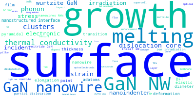
Help us to determine which of the papers that cite this potential actually used it to perform calculations. If you know, click the .
|
| Funding | Not available |
| Short KIM ID
The unique KIM identifier code.
| SM_333071728528_000 |
| Extended KIM ID
The long form of the KIM ID including a human readable prefix (100 characters max), two underscores, and the Short KIM ID. Extended KIM IDs can only contain alpha-numeric characters (letters and digits) and underscores and must begin with a letter.
| Sim_LAMMPS_Polymorphic_NordAlbeErhart_2003_GaN__SM_333071728528_000 |
| DOI |
10.25950/d947b5f4 https://doi.org/10.25950/d947b5f4 https://commons.datacite.org/doi.org/10.25950/d947b5f4 |
| KIM Item Type | Simulator Model |
| KIM API Version | 2.1 |
| Simulator Name
The name of the simulator as defined in kimspec.edn.
| LAMMPS |
| Potential Type | polymorphic |
| Simulator Potential | polymorphic |
| Run Compatibility | portable-models |
| Grade | Name | Category | Brief Description | Full Results | Aux File(s) |
|---|---|---|---|---|---|
| P | vc-species-supported-as-stated | mandatory | The model supports all species it claims to support; see full description. |
Results | Files |
| P | vc-periodicity-support | mandatory | Periodic boundary conditions are handled correctly; see full description. |
Results | Files |
| P | vc-permutation-symmetry | mandatory | Total energy and forces are unchanged when swapping atoms of the same species; see full description. |
Results | Files |
| B | vc-forces-numerical-derivative | consistency | Forces computed by the model agree with numerical derivatives of the energy; see full description. |
Results | Files |
| F | vc-dimer-continuity-c1 | informational | The energy versus separation relation of a pair of atoms is C1 continuous (i.e. the function and its first derivative are continuous); see full description. |
Results | Files |
| P | vc-objectivity | informational | Total energy is unchanged and forces transform correctly under rigid-body translation and rotation; see full description. |
Results | Files |
| P | vc-inversion-symmetry | informational | Total energy is unchanged and forces change sign when inverting a configuration through the origin; see full description. |
Results | Files |
| N/A | vc-memory-leak | informational | The model code does not have memory leaks (i.e. it releases all allocated memory at the end); see full description. |
Results | Files |
| N/A | vc-thread-safe | mandatory | The model returns the same energy and forces when computed in serial and when using parallel threads for a set of configurations. Note that this is not a guarantee of thread safety; see full description. |
Results | Files |
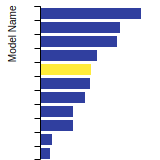
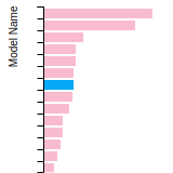
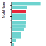
BCC Lattice Constant
This bar chart plot shows the mono-atomic body-centered cubic (bcc) lattice constant predicted by the current model (shown in the unique color) compared with the predictions for all other models in the OpenKIM Repository that support the species. The vertical bars show the average and standard deviation (one sigma) bounds for all model predictions. Graphs are generated for each species supported by the model.
Cohesive Energy Graph
This graph shows the cohesive energy versus volume-per-atom for the current mode for four mono-atomic cubic phases (body-centered cubic (bcc), face-centered cubic (fcc), simple cubic (sc), and diamond). The curve with the lowest minimum is the ground state of the crystal if stable. (The crystal structure is enforced in these calculations, so the phase may not be stable.) Graphs are generated for each species supported by the model.
(No matching species)Diamond Lattice Constant
This bar chart plot shows the mono-atomic face-centered diamond lattice constant predicted by the current model (shown in the unique color) compared with the predictions for all other models in the OpenKIM Repository that support the species. The vertical bars show the average and standard deviation (one sigma) bounds for all model predictions. Graphs are generated for each species supported by the model.
Dislocation Core Energies
This graph shows the dislocation core energy of a cubic crystal at zero temperature and pressure for a specific set of dislocation core cutoff radii. After obtaining the total energy of the system from conjugate gradient minimizations, non-singular, isotropic and anisotropic elasticity are applied to obtain the dislocation core energy for each of these supercells with different dipole distances. Graphs are generated for each species supported by the model.
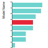
(No matching species)FCC Elastic Constants
This bar chart plot shows the mono-atomic face-centered cubic (fcc) elastic constants predicted by the current model (shown in blue) compared with the predictions for all other models in the OpenKIM Repository that support the species. The vertical bars show the average and standard deviation (one sigma) bounds for all model predictions. Graphs are generated for each species supported by the model.
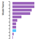
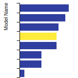
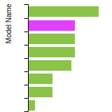
FCC Lattice Constant
This bar chart plot shows the mono-atomic face-centered cubic (fcc) lattice constant predicted by the current model (shown in red) compared with the predictions for all other models in the OpenKIM Repository that support the species. The vertical bars show the average and standard deviation (one sigma) bounds for all model predictions. Graphs are generated for each species supported by the model.
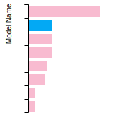
FCC Stacking Fault Energies
This bar chart plot shows the intrinsic and extrinsic stacking fault energies as well as the unstable stacking and unstable twinning energies for face-centered cubic (fcc) predicted by the current model (shown in blue) compared with the predictions for all other models in the OpenKIM Repository that support the species. The vertical bars show the average and standard deviation (one sigma) bounds for all model predictions. Graphs are generated for each species supported by the model.
(No matching species)FCC Surface Energies
This bar chart plot shows the mono-atomic face-centered cubic (fcc) relaxed surface energies predicted by the current model (shown in blue) compared with the predictions for all other models in the OpenKIM Repository that support the species. The vertical bars show the average and standard deviation (one sigma) bounds for all model predictions. Graphs are generated for each species supported by the model.
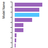
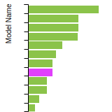
(No matching species)SC Lattice Constant
This bar chart plot shows the mono-atomic simple cubic (sc) lattice constant predicted by the current model (shown in the unique color) compared with the predictions for all other models in the OpenKIM Repository that support the species. The vertical bars show the average and standard deviation (one sigma) bounds for all model predictions. Graphs are generated for each species supported by the model.
Cubic Crystal Basic Properties Table
Species: GaSpecies: N
Creators: Junhao Li and Ellad Tadmor
Contributor: tadmor
Publication Year: 2019
DOI: https://doi.org/10.25950/49c5c255
Computes the cubic elastic constants for some common crystal types (fcc, bcc, sc, diamond) by calculating the hessian of the energy density with respect to strain. An estimate of the error associated with the numerical differentiation performed is reported.
| Test | Test Results | Link to Test Results page | Benchmark time
Usertime multiplied by the Whetstone Benchmark. This number can be used (approximately) to compare the performance of different models independently of the architecture on which the test was run.
Measured in Millions of Whetstone Instructions (MWI) |
|---|---|---|---|
| Elastic constants for bcc N at zero temperature v005 | view | 3946 | |
| Elastic constants for diamond N at zero temperature v000 | view | 16524 | |
| Elastic constants for fcc N at zero temperature v005 | view | 4652 | |
| Elastic constants for sc N at zero temperature v005 | view | 3690 |
Creators: Junhao Li and Ellad Tadmor
Contributor: tadmor
Publication Year: 2019
DOI: https://doi.org/10.25950/5853fb8f
Computes the cubic elastic constants for some common crystal types (fcc, bcc, sc, diamond) by calculating the hessian of the energy density with respect to strain. An estimate of the error associated with the numerical differentiation performed is reported.
| Test | Test Results | Link to Test Results page | Benchmark time
Usertime multiplied by the Whetstone Benchmark. This number can be used (approximately) to compare the performance of different models independently of the architecture on which the test was run.
Measured in Millions of Whetstone Instructions (MWI) |
|---|---|---|---|
| Elastic constants for bcc Ga at zero temperature v006 | view | 9565 | |
| Elastic constants for diamond Ga at zero temperature v001 | view | 7581 | |
| Elastic constants for fcc Ga at zero temperature v006 | view | 2911 | |
| Elastic constants for sc Ga at zero temperature v006 | view | 9245 |
Creators: Junhao Li
Contributor: jl2922
Publication Year: 2018
DOI: https://doi.org/10.25950/2e4b93d9
Computes the elastic constants for hcp crystals by calculating the hessian of the energy density with respect to strain. An estimate of the error associated with the numerical differentiation performed is reported.
| Test | Test Results | Link to Test Results page | Benchmark time
Usertime multiplied by the Whetstone Benchmark. This number can be used (approximately) to compare the performance of different models independently of the architecture on which the test was run.
Measured in Millions of Whetstone Instructions (MWI) |
|---|---|---|---|
| Elastic constants for hcp Ga at zero temperature | view | 2031 | |
| Elastic constants for hcp N at zero temperature | view | 1612 |
Creators:
Contributor: ilia
Publication Year: 2024
DOI: https://doi.org/10.25950/2f2c4ad3
Computes the equilibrium crystal structure and energy for an arbitrary crystal at zero temperature and applied stress by performing symmetry-constrained relaxation. The crystal structure is specified using the AFLOW prototype designation. Multiple sets of free parameters corresponding to the crystal prototype may be specified as initial guesses for structure optimization. No guarantee is made regarding the stability of computed equilibria, nor that any are the ground state.
Creators:
Contributor: ilia
Publication Year: 2025
DOI: https://doi.org/10.25950/866c7cfa
Computes the equilibrium crystal structure and energy for an arbitrary crystal at zero temperature and applied stress by performing symmetry-constrained relaxation. The crystal structure is specified using the AFLOW prototype designation. Multiple sets of free parameters corresponding to the crystal prototype may be specified as initial guesses for structure optimization. No guarantee is made regarding the stability of computed equilibria, nor that any are the ground state.
| Test | Test Results | Link to Test Results page | Benchmark time
Usertime multiplied by the Whetstone Benchmark. This number can be used (approximately) to compare the performance of different models independently of the architecture on which the test was run.
Measured in Millions of Whetstone Instructions (MWI) |
|---|---|---|---|
| Equilibrium crystal structure and energy for Ga in AFLOW crystal prototype A_cI12_220_a v003 | view | 253102 | |
| Equilibrium crystal structure and energy for Ga in AFLOW crystal prototype A_oC40_63_2cf3g v003 | view | 684522 | |
| Equilibrium crystal structure and energy for Ga in AFLOW crystal prototype A_oC4_63_c v003 | view | 163444 | |
| Equilibrium crystal structure and energy for Ga in AFLOW crystal prototype A_oC8_63_g v003 | view | 206827 | |
| Equilibrium crystal structure and energy for Ga in AFLOW crystal prototype A_oC8_64_f v003 | view | 246376 | |
| Equilibrium crystal structure and energy for Ga in AFLOW crystal prototype A_tI2_139_a v003 | view | 183799 |
Creators: Daniel S. Karls and Junhao Li
Contributor: karls
Publication Year: 2019
DOI: https://doi.org/10.25950/2765e3bf
Equilibrium lattice constant and cohesive energy of a cubic lattice at zero temperature and pressure.
| Test | Test Results | Link to Test Results page | Benchmark time
Usertime multiplied by the Whetstone Benchmark. This number can be used (approximately) to compare the performance of different models independently of the architecture on which the test was run.
Measured in Millions of Whetstone Instructions (MWI) |
|---|---|---|---|
| Equilibrium zero-temperature lattice constant for bcc Ga v007 | view | 4990 | |
| Equilibrium zero-temperature lattice constant for bcc N v007 | view | 6782 | |
| Equilibrium zero-temperature lattice constant for diamond Ga v007 | view | 8701 | |
| Equilibrium zero-temperature lattice constant for diamond N v007 | view | 6750 | |
| Equilibrium zero-temperature lattice constant for fcc Ga v007 | view | 7773 | |
| Equilibrium zero-temperature lattice constant for fcc N v007 | view | 5438 | |
| Equilibrium zero-temperature lattice constant for sc Ga v007 | view | 5694 | |
| Equilibrium zero-temperature lattice constant for sc N v007 | view | 7262 |
Creators: Junhao Li
Contributor: jl2922
Publication Year: 2018
DOI: https://doi.org/10.25950/25bcc28b
Calculates lattice constant of hexagonal bulk structures at zero temperature and pressure by using simplex minimization to minimize the potential energy.
| Test | Test Results | Link to Test Results page | Benchmark time
Usertime multiplied by the Whetstone Benchmark. This number can be used (approximately) to compare the performance of different models independently of the architecture on which the test was run.
Measured in Millions of Whetstone Instructions (MWI) |
|---|---|---|---|
| Equilibrium lattice constants for hcp Ga | view | 8512 | |
| Equilibrium lattice constants for hcp N | view | 10125 |
| Test | Error Categories | Link to Error page |
|---|---|---|
| Cohesive energy versus lattice constant curve for bcc Nitrogen | other | view |
| Cohesive energy versus lattice constant curve for diamond Nitrogen | other | view |
| Cohesive energy versus lattice constant curve for fcc Nitrogen | other | view |
| Cohesive energy versus lattice constant curve for sc Nitrogen | other | view |
CohesiveEnergyVsLatticeConstant__TD_554653289799_003
| Test | Error Categories | Link to Error page |
|---|---|---|
| Cohesive energy versus lattice constant curve for bcc Ga v004 | other | view |
| Cohesive energy versus lattice constant curve for diamond Ga v003 | other | view |
| Cohesive energy versus lattice constant curve for fcc Ga v003 | other | view |
| Cohesive energy versus lattice constant curve for sc Ga v003 | other | view |
EquilibriumCrystalStructure__TD_457028483760_000
| Test | Error Categories | Link to Error page |
|---|---|---|
| Equilibrium crystal structure and energy for N in AFLOW crystal prototype A_hP2_194_c v000 | other | view |
| Equilibrium crystal structure and energy for N in AFLOW crystal prototype A_hR16_167_cf v000 | other | view |
EquilibriumCrystalStructure__TD_457028483760_003
| Test | Error Categories | Link to Error page |
|---|---|---|
| Equilibrium crystal structure and energy for Ga in AFLOW crystal prototype A_mC2_12_a v003 | other | view |
| Equilibrium crystal structure and energy for Ga in AFLOW crystal prototype A_mC4_15_e v003 | other | view |
LatticeConstantCubicEnergy__TD_475411767977_007
| Test | Error Categories | Link to Error page |
|---|---|---|
| Equilibrium zero-temperature lattice constant for bcc N v007 | other | view |
| Equilibrium zero-temperature lattice constant for diamond N v007 | other | view |
| Equilibrium zero-temperature lattice constant for fcc N v007 | other | view |
| Equilibrium zero-temperature lattice constant for sc N v007 | other | view |
LatticeConstantHexagonalEnergy__TD_942334626465_005
| Test | Error Categories | Link to Error page |
|---|---|---|
| Equilibrium lattice constants for hcp Ga v005 | other | view |
| Equilibrium lattice constants for hcp N v005 | other | view |
| Sim_LAMMPS_Polymorphic_NordAlbeErhart_2003_GaN__SM_333071728528_000.txz | Tar+XZ | Linux and OS X archive |
| Sim_LAMMPS_Polymorphic_NordAlbeErhart_2003_GaN__SM_333071728528_000.zip | Zip | Windows archive |